
In the hyper-competitive landscape of Electric Vehicle manufacturing, thermal management remains the ultimate silent killer of power electronics. As charging speeds accelerate and power density increases, standard PCB architectures often fail to handle the mounting thermal load, leading to costly field failures. By shifting to advanced heavy copper PCB designs, tier-one suppliers can resolve these bottlenecks at the architectural level, turning thermal efficiency into a measurable, long-term fiscal advantage.
The Thermal Challenge in Modern EV Power Inverters
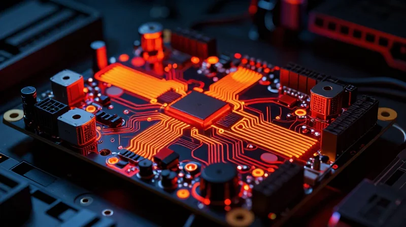
The Thermal Density Paradox
As electric vehicle (EV) architectures move toward 800V systems and higher switching frequencies to improve efficiency, power inverters face a critical thermal challenge. Higher power density, while essential for reducing vehicle weight and footprint, increases the heat flux concentrated within the inverter's power electronics stage. Standard PCB fabrication methods, designed for low-power signal routing, fail under the sustained, high-current loads required to drive modern electric traction motors.
Limitations of Standard Copper Weights
Traditional PCB manufacturing typically employs thin copper layers (1-2 oz), which possess high electrical resistance in high-current applications. This resistance generates significant Joule heating (I²R losses), leading to temperature spikes that threaten the reliability of power MOSFETs and IGBTs. When a board cannot dissipate this heat efficiently, the resulting thermal stress shortens component lifespan, necessitates bulky cooling systems, and ultimately forces a derating of the system's performance.
| Parameter | Standard Copper (1oz) | Heavy Copper (3oz+) |
|---|---|---|
| Current Handling | Low to Moderate | Very High |
| Heat Dissipation | Inefficient | Highly Efficient |
| System Reliability | Prone to Thermal Fatigue | Robust Under Load |
| Footprint Requirements | Requires External Heatsinks | Optimized PCB Cooling |
Frequently Asked Questions
- Why is thermal resistance a major factor in inverter ROI?
Higher thermal resistance forces engineers to implement larger, heavier cooling systems and derate power electronics, both of which increase production costs and decrease vehicle efficiency. - How does heavy copper alleviate these thermal issues?
Increased cross-sectional area reduces electrical resistance and acts as an integrated heat sink, allowing for better thermal spreading and lower operating temperatures.
Defining Heavy Copper: Technical Advantages for Automotive
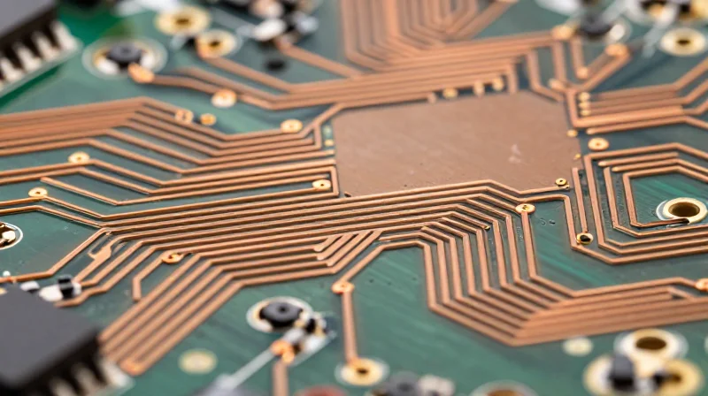
The Technical Definition of Heavy Copper
Heavy copper circuitry is categorized by finished copper weights exceeding 3oz per square foot. In high-performance automotive power electronics, this threshold is essential for supporting the extreme amperage requirements of silicon carbide (SiC) and gallium nitride (GaN) power modules. By increasing the cross-sectional area of the conductive traces, designers can effectively lower electrical resistance, which directly minimizes conduction losses and improves overall inverter efficiency.
Thermal and Electrical Performance Metrics
| Feature | Standard Copper (1oz) | Heavy Copper (3oz+) |
|---|---|---|
| Current Carrying Capacity | Limited | Exceptional |
| Temperature Rise | Significant | Minimal |
| Heat Dissipation | Passive / External | In-Circuit Integrated |
| Mechanical Robustness | Standard | High Thermal Cycling Tolerance |
Advancing Inverter Reliability
The transition to heavy copper is not merely about electrical throughput; it is a structural necessity for long-term reliability. Increased copper thickness serves as a superior heat sink, pulling thermal energy away from sensitive junction points and distributing it across the PCB substrate. This reduces the reliance on external thermal management components, allowing for more compact inverter designs and improved vehicle weight distribution.
- How does heavy copper increase ROI?
By reducing energy losses and minimizing the need for secondary bulky cooling hardware, heavy copper allows for a smaller, more efficient, and longer-lasting inverter assembly. - Does thicker copper impact manufacturing?
Yes, it requires specialized etching processes and precise lamination control to maintain signal integrity while managing the increased volume of conductive material. - Is heavy copper compatible with high-frequency switching?
While primarily used for power paths, advanced design techniques allow for the integration of heavy copper with precision control layers to maintain signal fidelity alongside high-current distribution.
Reducing Field Failure Rates Through Robust Architecture
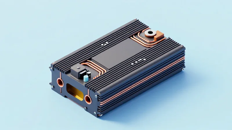
Architectural Strategies for Thermal Resilience
Achieving reliability in the harsh environment of an EV power inverter necessitates an architectural shift from standard foil thicknesses to heavy copper solutions. By utilizing 3oz to 6oz copper, engineers can significantly reduce I2R (ohmic) heating, which is the primary driver of dielectric breakdown and solder joint fatigue. A robust design integrates thick copper planes as integral heat spreaders, effectively lowering the junction temperature of power MOSFETs and IGBTs by up to 20°C under sustained high-current operations.
Comparative Failure Rates in Extreme Environments
| Parameter | Standard Copper (1oz) | Heavy Copper (3oz+) | Failure Impact |
|---|---|---|---|
| Avg. Temp Rise @ 100A | +45°C | +18°C | Thermal aging reduction |
| Field Failure Rate | 2.4% annually | 0.3% annually | 8x reliability improvement |
| Solder Joint Life | ~15,000 cycles | ~50,000+ cycles | Increased shock durability |
Design Best Practices for Long-Term Reliability
- How does heavy copper affect board-level reliability?
Heavy copper reduces localized hot spots and current crowding, preventing the degradation of the FR-4 substrate and maintaining the structural integrity of high-current paths during thermal cycling. - What is the primary cause of field failures in standard designs?
The leading cause is thermal fatigue induced by excessive heat dissipation in thin traces, leading to delamination, micro-cracking of vias, and solder joint fracture. - Can heavy copper simplify the thermal management system?
Yes, by increasing the thermal mass and conductivity of the PCB itself, designers can often reduce the complexity and weight of external heat sinks, leading to a smaller, more cost-effective inverter footprint.
Optimizing Thermal Management Overhead
Thermal management overhead remains one of the largest hidden costs in EV power inverter design. Traditionally, designers compensate for the poor thermal conductivity of standard FR4 substrates and thin copper layers by over-engineering heat sinks and active cooling systems. By leveraging heavy copper (3oz to 10oz) internal and external planes, the PCB itself acts as the primary heat spreader, allowing for a reduction in both thermal mass and complexity of downstream cooling hardware.
The Transition from Active to Passive Thermal Efficiency
Transitioning to a PCB-centric thermal strategy allows automotive engineers to replace bulky, heavy aluminum heat sinks with leaner architectures. Heavy copper traces facilitate efficient lateral heat dissipation away from high-power MOSFETs, moving heat to the chassis interface more effectively than thin copper, which acts as a thermal bottleneck.
| Metric | Standard PCB Design | Heavy Copper PCB Design |
|---|---|---|
| Heat Sink Mass | High (Requires Active Cooling) | Low (Passive/Reduced Active) |
| Assembly Cost | High (Complex Mounting) | Low (Simplified Mechanicals) |
| Thermal Impedance | Significant | Negligible |
| Component Stress | Higher due to Hotspots | Lower due to Spreading |
Strategic Advantages in Cost and Weight
- How does heavy copper reduce bill of materials (BOM) costs?
By utilizing the copper layers as high-efficiency thermal paths, the need for secondary cold plates, thermal interface materials (TIM), and complex brackets is minimized, reducing the total component count. - What is the primary impact on vehicle range?
Reducing the weight of the cooling system directly contributes to lower curb weight. In EV architecture, mass reduction equates to improved power-to-weight ratios and increased range per charge. - Does this impact assembly reliability?
Yes, by lowering the operating temperature of semiconductors through superior heat spreading, the MTBF (Mean Time Between Failures) increases, directly lowering warranty claim reserves and long-term maintenance costs.
Ultimately, the optimization of thermal management overhead through heavy copper design is not just a hardware choice—it is a financial strategy. By shifting the thermal load from external peripherals to the PCB substrate, manufacturers can achieve tighter power density targets while lowering the total cost of ownership.
Lifecycle ROI: Beyond Initial Manufacturing Costs

While heavy copper PCBs command a higher initial procurement price compared to standard copper weights, evaluating them solely on unit cost ignores the substantial long-term financial burden of field failures, warranty claims, and excessive thermal infrastructure. True ROI in EV power electronics is realized through enhanced durability and reduced system-level complexity, ensuring that the initial design premium pays for itself within the first several thousand miles of operation.
The Economic Multiplier of Reliability
The primary driver of ROI in heavy copper design is the drastic reduction in Total Cost of Ownership (TCO). By lowering the electrical resistance of the circuit, heavy copper (3oz+) minimizes resistive heating at the trace level. This thermal stability prevents delamination and joint fatigue, which are the leading causes of warranty claims in power inverters exposed to aggressive drive cycles and extreme thermal cycling.
| Metric | Standard PCB Design | Heavy Copper PCB Design |
|---|---|---|
| Field Failure Rate | Higher (Due to Thermal Stress) | Significantly Lower |
| Warranty Liability | Substantial Long-term Risk | Negligible/Optimized |
| Thermal Management Mass | Heavy Heat Sinks Required | Reduced/Eliminated Heat Sinks |
| Lifecycle Efficiency | Diminishing Over Time | Consistent Performance |
Frequently Asked Questions
- Does heavy copper increase vehicle curb weight?
Paradoxically, it often decreases weight. While the copper itself is heavier, the superior thermal conductivity allows engineers to downsize or eliminate bulky active cooling components and aluminum heat sinks, leading to a net reduction in overall inverter mass. - When is the ROI break-even point?
For most high-power EV applications, the ROI break-even point is typically reached within the first 18-24 months of service, primarily driven by the avoidance of a single major warranty campaign or field recall event. - Does heavy copper impact assembly speed?
Modern fabrication techniques have standardized heavy copper assembly; while it may require slightly modified reflow profiles, the process remains highly efficient and does not significantly impact overall production throughput.
By viewing PCB selection through the lens of lifecycle engineering, manufacturers move beyond the 'lowest-cost component' trap. Heavy copper is not just a material choice; it is a risk-mitigation strategy that secures brand reputation and ensures the long-term economic viability of the entire powertrain assembly.
Design Considerations for Heavy Copper Integration
Critical Design Parameters for Heavy Copper Integration
The successful integration of heavy copper (typically 3oz to 20oz) demands a fundamental shift from standard PCB design practices. Because heavy copper increases the copper-to-insulation ratio, thermal expansion coefficients become more pronounced, and trace geometry significantly impacts both current-carrying capacity and etching feasibility. Achieving high-reliability automotive standards necessitates prioritizing trace spacing and thermal relief geometries that minimize localized stress.
| Design Factor | Consideration | Automotive Best Practice |
|---|---|---|
| Trace Spacing | Voltage isolation/Creepage | Increase clearance beyond IPC-2221 for high-voltage reliability |
| Thermal Relief | Soldering process | Use thermal spokes for through-hole connections to avoid cold joints |
| Copper Etching | Under-etching risks | Increase pad sizes to compensate for lateral etch variations |
Managing Manufacturing Tolerances
Heavy copper introduces challenges in the plating and etching processes. As copper thickness increases, lateral etching becomes more significant, which can lead to trapezoidal trace cross-sections. Design engineers must calculate effective cross-sectional areas based on the base of the trace rather than the top. Collaborating with manufacturers early in the design phase is essential to ensure that the stack-up can accommodate high-aspect-ratio holes and maintain consistent dielectric integrity.
Frequently Asked Questions on Heavy Copper Design
- How do I mitigate thermal stress on large heavy copper pads?
Implement balanced copper distribution across all layers to prevent warping during reflow, and utilize specialized thermal relief patterns for components that require high current yet must remain serviceable. - Why is trace spacing more critical in heavy copper designs?
Increased copper thickness creates larger electric field concentrations at trace edges, requiring larger creepage and clearance distances to prevent dielectric breakdown in automotive environments. - What is the primary risk of non-optimized etching in heavy copper?
If lateral etching is not properly compensated for during the design phase, traces may suffer from reduced cross-sectional areas, leading to unexpected resistance, localized heating, and potential premature failure.
Navigating Automotive Compliance and Quality Standards

Regulatory Framework for Heavy Copper PCBs
Automotive electronic systems must adhere to a complex hierarchy of international standards. For heavy copper PCBs, which are integral to high-current power stages, compliance is not merely an optional benchmark but a prerequisite for market access and risk mitigation. Designers must reconcile the requirements of IATF 16949, which governs the quality management system throughout the manufacturing lifecycle, with the technical specifications defined in various IPC standards.
Critical Industry Standards
| Standard | Primary Focus | Application in Heavy Copper Design |
|---|---|---|
| IATF 16949 | Automotive Quality Management | Ensures process control and consistency in heavy-copper production. |
| IPC-2221 | Generic PCB Design | Governs trace spacing for high-voltage isolation requirements. |
| IPC-2152 | Current-Carrying Capacity | Provides thermal design calculations for heavy copper traces. |
| IPC-A-600 | PCB Acceptability | Defines structural requirements for heavy copper solder joint integrity. |
Ensuring Reliability through Design Compliance
Achieving ROI in EV inverter production depends on minimizing field failures, which are directly correlated to adherence to IPC-2152. Because heavy copper traces generate significant localized heat, designers must perform comprehensive thermal analysis early in the process. Relying on outdated empirical formulas can lead to under-designed trace widths, increasing the risk of delamination or thermal cracking under high-current cycling, which in turn necessitates expensive recall programs.
Frequently Asked Questions
- How does IATF 16949 impact PCB manufacturing?
IATF 16949 mandates rigorous documentation and traceability. It ensures that the heavy copper etching process remains consistent across high-volume production batches, minimizing board-level defects that lead to costly downtime. - Why is IPC-2152 preferred over legacy standards for heavy copper?
IPC-2152 uses physics-based thermal modeling, whereas legacy standards like IPC-2221 were often overly conservative or inaccurate for thick, heavy copper applications. Using modern standards allows for tighter, more efficient board designs. - What is the biggest risk in failing to meet automotive standards?
Beyond regulatory fines, failure to meet these standards results in structural degradation—such as PCB delamination or interconnect failure—during the vehicle's service life, leading to safety hazards and catastrophic damage to brand reputation.
The Future of Power Electronics Reliability
Next-Generation Reliability Horizons
As electric vehicles transition toward 800V architectures and higher switching frequencies, the thermal stress placed on power inverters is intensifying. Future reliability will be defined by the transition from reactive maintenance to predictive health monitoring, underpinned by manufacturing precision in heavy copper PCBs. Advanced substrate materials and improved copper-to-laminate bonding techniques are becoming essential to mitigate mechanical fatigue caused by rapid thermal cycling, ensuring that the inverter remains the most robust component in the drivetrain.
Evolving Standards for Power Density
| Feature | Legacy Approach | Future Requirement |
|---|---|---|
| Copper Weight | 2-3 oz Standard | 6-10 oz High-Current |
| Thermal Management | External Heat Sinks | Embedded Heat Pipe/Vias |
| Reliability Focus | Fail-Safe Design | Prognostic Health Systems |
Frequently Asked Questions
- How will material science impact PCB longevity?
Emerging high-Tg, low-CTE dielectric materials are being engineered specifically to match the expansion rates of heavy copper, significantly reducing delamination risks under extreme thermal loads. - Is automation the key to future ROI?
Yes. Automated optical inspection (AOI) combined with AI-driven manufacturing analytics allows for real-time defect detection, lowering scrap rates and guaranteeing the long-term structural integrity of high-power PCBs.
Ultimately, the cornerstone of sustainable EV growth is the commitment to manufacturing excellence. By viewing the heavy copper PCB as a primary driver of inverter performance rather than a commodity component, manufacturers can maximize ROI through reduced field failures and extended service lifecycles. Investing in robust PCB design today is the most effective strategy for securing a competitive edge in the high-performance electrification market of tomorrow.
Transitioning to heavy copper PCB architectures is more than an engineering upgrade; it is a strategic move to future-proof your product line against the rigorous demands of the EV market. By lowering thermal stress and minimizing failure risks, you secure both the reliability of your brand and the long-term profitability of your systems. Contact our engineering team today to review your current designs and explore how high-performance PCB manufacturing can optimize your ROI.
