
In the fast-evolving world of digital cockpits and industrial dashboards, the printed circuit board is the unsung hero. As displays grow larger and resolutions sharpen, engineers face unprecedented thermal and signal integrity challenges. This guide provides the strategic blueprint for selecting materials and layouts that guarantee your hardware stands the test of time.
The Unique Challenges of Large-Format Display PCBs
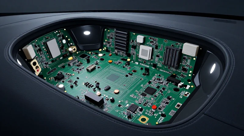
The Mechanical Dilemma of Oversized Substrates
As automotive display technology migrates toward panoramic cockpit configurations, PCBs are transitioning from traditional compact footprints to large-format, high-aspect-ratio substrates. This increase in dimensions fundamentally alters the mechanical behavior of the board. The primary challenge lies in minimizing warpage during the reflow soldering process. Larger PCBs possess a higher susceptibility to thermal expansion, which can lead to solder joint fatigue, via cracking, and microscopic delamination if the coefficient of thermal expansion (CTE) is not meticulously balanced between the substrate material and the copper circuitry.
Thermal Management in High-Density Environments
High pixel density demands elevated power delivery, which in turn creates localized thermal hotspots that are difficult to dissipate across a single large board. Unlike smaller boards that may benefit from natural chassis cooling, large-format PCBs often suffer from uneven heat distribution. Engineers must implement advanced thermal vias and integrated heat-spreading copper planes to prevent degradation of sensitive display driver ICs.
| Challenge Factor | Impact on Large-Format PCB | Mitigation Strategy |
|---|---|---|
| Mechanical Warpage | Potential solder joint failure | High-Tg materials, stiffener ribs |
| Thermal Density | Component localized degradation | Thermal vias, heavy copper layers |
| Signal Integrity | EMI/EMC radiation risk | Multi-layer shielding, impedance control |
Key Engineering FAQs
- How does substrate size affect assembly yields?
Increased surface area heightens the risk of bowing in the oven, necessitating optimized reflow profiles and custom carrier fixtures to maintain coplanarity. - Can standard FR-4 material support large-format clusters?
While possible for simple designs, high-performance clusters usually require hybrid laminates or high-glass-transition temperature (Tg) materials to withstand the stresses of high-density mounting. - Why is board thickness critical for large PCBs?
A thicker board offers greater mechanical rigidity but adds weight and complicates thermal flow; the selection must balance stiffness against thermal mass requirements.
Selecting the Ideal Substrate for Dimensional Stability
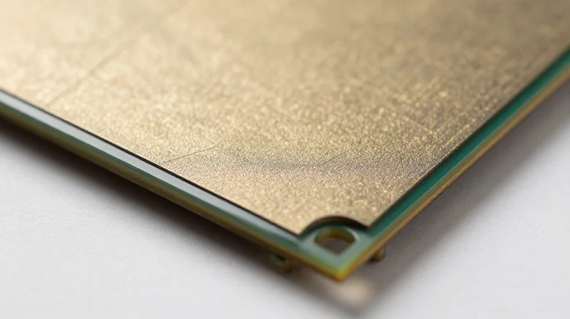
For large-format PCB arrays, the substrate acts as the primary defense against mechanical failure. As dimensions increase, the coefficient of thermal expansion (CTE) becomes the most significant factor in maintaining dimensional stability. Choosing a material that matches your assembly's thermal requirements is not merely a design preference; it is a fundamental requirement to ensure display alignment and prevent solder joint fatigue.
Material Performance Comparison
| Material Class | Primary Advantage | Best Use Case |
|---|---|---|
| High-Tg FR-4 | Cost-effective stability | Standard automotive clusters |
| Polyimide | High-flex & heat resistance | Complex curved displays |
| Ceramic-Filled PTFE | Ultra-low CTE | High-power dense backplanes |
Key Considerations for Substrate Selection
- Why is Tg (Glass Transition Temperature) critical for large boards?
A higher Tg ensures the material remains rigid during reflow processes and thermal cycling, preventing the PCB from bowing or twisting as temperatures fluctuate within the instrument cabin. - How does substrate thickness impact dimensional stability?
Thicker boards offer increased inherent stiffness, which can help resist warping. However, this must be balanced against the weight constraints and spatial limitations of the dashboard housing. - Are there specific advantages to metal-core boards?
For high-brightness displays generating significant heat, metal-core substrates provide superior thermal dissipation compared to traditional laminates, drastically reducing localized hotspots that lead to mechanical distortion.
Ultimately, the selection process requires evaluating the board's operational environment. For automotive-grade instrument clusters, we recommend prioritizing laminates with a Tg above 170°C and a low-CTE glass reinforcement (like low-CTE weave) to ensure that even at extreme thermal thresholds, the display interface remains perfectly planar.
Advanced Thermal Management Strategies

Advanced Thermal Management Strategies
In high-resolution instrument clusters, thermal management is not merely an auxiliary concern; it is a fundamental pillar of hardware reliability. As display drivers and SoCs push higher frame rates and resolutions, the localized heat density can lead to substrate degradation, signal timing shifts, and premature component failure. Implementing a multi-layered thermal strategy—balancing conductive paths, structural thermal vias, and external coupling—is essential for sustaining peak performance in confined automotive environments.
Heat Dissipation Techniques Comparison
| Strategy | Primary Function | Implementation Complexity |
|---|---|---|
| Copper Pours (Heavy Copper) | Spreads thermal energy across surface area | Low |
| Thermal Via Arrays | Conducts heat to inner layers/bottom side | Moderate |
| Heat Sink Coupling | Dissipates heat to chassis/ambient air | High |
Thermal Strategy FAQ
- How do thermal vias influence signal integrity in high-speed designs?
While essential for cooling, dense thermal via arrays create discontinuities in the return path. Designers must perform impedance modeling to ensure that thermal via placement does not introduce excessive crosstalk or ground bounce in high-speed digital lines. - What role does heavy copper play in large-format PCB stability?
Beyond thermal conductivity, increasing copper weight—such as using 2oz or 3oz copper—adds structural rigidity to the PCB, which is critical for preventing warping in large-format substrates under thermal cycling. - Is direct heat sink contact with components always recommended?
Not necessarily. For advanced clusters, using a Thermal Interface Material (TIM) between the SoC and the heat sink is preferred to account for Coefficient of Thermal Expansion (CTE) mismatches that could otherwise fracture solder joints during vehicle cold-cranking cycles.
The integration of these strategies requires a cohesive approach. Ensure that your PCB design includes dedicated thermal planes that remain contiguous across the board layout to avoid 'heat islands.' Furthermore, prioritize the placement of high-wattage drivers near mechanical mounting points that can serve as secondary heat sinks to the vehicle chassis.
Maintaining Signal Integrity at Scale
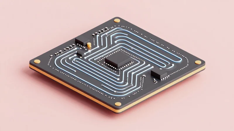
Strategies for High-Speed Differential Pairs
In expansive display layouts, high-speed signals—such as LVDS or FPD-Link—are susceptible to skew and impedance discontinuities over long traces. Maintaining signal integrity requires rigorous adherence to controlled-impedance design, typically 100 ohms for differential pairs. Designers must ensure strict length matching (trace-to-trace) to minimize skew, and utilize 'stitching vias' along return paths to keep the loop area as small as possible.
EMI Mitigation in Large-Format Architectures
Large-format boards act as significant radiators for electromagnetic interference (EMI). To minimize this, prioritize a solid ground plane strategy and the strategic placement of decoupling capacitors close to high-speed IC power pins. For edge-to-edge communication, use via fences to contain high-frequency noise within the signal layers.
| Technique | Primary Benefit | Implementation Tip |
|---|---|---|
| Via Fencing | EMI Containment | Space vias at 1/10th of the signal wavelength. |
| Back-drilling | Signal Integrity | Remove stubs to prevent resonance at high frequencies. |
| Differential Shielding | Crosstalk Reduction | Increase clearance between adjacent high-speed pairs. |
Frequently Asked Questions
- How does PCB size affect signal propagation?
Increased trace lengths lead to higher insertion loss and dielectric absorption. Use lower-loss materials and optimize trace width/spacing to maintain signal eye diagrams. - Is a six-layer stack-up sufficient for large instrument clusters?
Usually insufficient. Larger designs typically require 8 to 12 layers to ensure dedicated ground/power planes that isolate high-speed digital signals from noise-sensitive analog components.
Layer Stack-up Optimization for Performance
In the context of advanced instrument clusters, the PCB stack-up is the fundamental architecture that dictates both mechanical reliability and electrical performance. For large-format boards, achieving a balanced, symmetric structure is critical to preventing thermal-induced warpage during the reflow process and ensuring consistent impedance control across the expansive surface area.
Symmetry and Warpage Mitigation
Large-format boards are highly susceptible to bowing and twisting due to asymmetric copper distribution. Designers must prioritize balance in both the Z-axis (layer stack) and the X-Y plane (copper weight distribution). Maintaining an equal number of layers on either side of the neutral axis, using identical copper weights, and utilizing balanced prepreg styles are mandatory practices to ensure dimensional stability.
| Design Factor | Best Practice for Large Format | Impact on Performance |
|---|---|---|
| Copper Distribution | Balanced copper weight per layer | Reduces stress-induced warpage |
| Dielectric Material | Symmetric core/prepreg construction | Ensures uniform thermal expansion |
| Layer Sequencing | Mirror-image stack-up design | Improves dimensional stability |
Enhancing Routing Density
To support the dense interconnects required for high-resolution displays and real-time processing in instrument clusters, optimization of the layer stack is essential. Implementing HDI (High-Density Interconnect) techniques, such as blind and buried vias, allows for higher trace density without compromising signal integrity or ground plane continuity.
- How does stack-up symmetry affect reliability?
Symmetry ensures that thermal expansion forces are equalized across the board, preventing mechanical stress that leads to solder joint fractures and PCB bowing. - When should I consider HDI technologies?
HDI should be utilized when the complexity of the cluster's GPU or SoC requires advanced fan-out patterns that exceed the routing capabilities of standard through-hole designs. - What role do reference planes play?
Proper reference planes are essential for maintaining constant impedance; they provide the necessary return paths for high-speed signals, minimizing electromagnetic interference (EMI) across the large-scale layout.
Mitigating Mechanical Stress and Vibration

In large-format instrument clusters, mechanical stress is the primary driver of solder joint fatigue and interlayer delamination. Because these PCBs cover a significant surface area, they act as mechanical levers; even minor chassis vibrations can amplify stress at the periphery and near stiff components. Engineers must treat the PCB as a structural member rather than a simple carrier of circuitry.
Designing for Structural Rigidity and Mounting
The fundamental goal is to increase the resonant frequency of the PCB assembly to avoid harmonic coupling with the vehicle's operational vibration profiles. Increasing board thickness is a common starting point, but it must be balanced against weight constraints.
- Strategic Mounting Points
Locate mounting holes near high-mass components to minimize cantilever effects. Avoid placing mounting holes near delicate BGA or high-density connectors where chassis flex could induce stress. - Damping Interfaces
Utilize elastomeric grommets or standoffs at mounting points to provide a mechanical filter that attenuates high-frequency vibration before it reaches the laminate. - Board Thickness Selection
Standard 1.6mm boards often suffer from excessive deflection in large formats. Upgrade to 2.4mm or 3.2mm substrates for larger clusters to reduce sag and improve mounting stability.
Component Placement and Solder Joint Reliability
| Strategy | Action | Impact |
|---|---|---|
| Component Orientation | Align long axis with stress profile | Reduces solder joint lever arm torque |
| Underfill Application | Apply epoxy to high-mass parts | Distributes thermal/mechanical strain |
| Corner Bonding | Adhesive dots on package corners | Prevents premature BGA solder fatigue |
Best Practices for Harsh Environment Resilience
To finalize the design, implement a keep-out zone policy. Keep all surface-mount components at least 5mm away from board edges, especially near mounting points, to prevent damage caused by board strain during installation or operational thermal cycling. Additionally, ensure that all heavy components, such as inductors or electrolytic capacitors, are mechanically anchored with thermally conductive adhesives to prevent vibration-induced separation from the solder pads.
Ensuring Reliability through Rigorous Testing
For advanced automotive and industrial instrument clusters, a 'design-to-fail' testing mindset is required. Large-format PCBs are inherently more susceptible to physical stress and signal degradation, making standardized validation protocols the only defense against zero-defect failures in the field.
Core Validation Protocols for Large-Format Boards
| Test Category | Primary Goal | Metric for Success |
|---|---|---|
| Thermal Cycling | Identify CTE mismatch failures | Zero impedance drift over 500 cycles |
| Vibration/Shock | Validate solder joint integrity | No intermittent continuity loss |
| Signal Integrity | Ensure high-speed data fidelity | Eye-diagram mask compliance |
Frequently Asked Questions Regarding PCB Reliability
- Why is thermal cycling critical for large-format PCBs?
Large boards suffer from non-uniform thermal expansion. Testing across temperature extremes ensures that the coefficients of thermal expansion (CTE) of the laminate and copper layers do not induce delamination or micro-cracking. - What role does vibration testing play in component placement?
Vibration testing exposes potential resonances. For large PCBs, this helps identify areas where heavier components (like power inductors) act as leverage points, requiring additional adhesive or mechanical anchoring. - How do we ensure long-term signal integrity?
By performing TDR (Time Domain Reflectometry) analysis before and after environmental stress testing, we can verify that the interconnects remain stable and that no impedance discontinuities have emerged.
Ultimately, reliability is not a post-production check but a continuous requirement. Integrate HALT (Highly Accelerated Life Testing) early in the prototyping phase to identify failure modes before moving to full-scale production.
Selecting the right large-format PCB is not merely a design task but a long-term reliability investment. By focusing on substrate quality, thermal efficiency, and signal integrity, you can ensure your instrument clusters perform flawlessly in any condition. Ready to optimize your hardware roadmap? Contact our engineering team today for a consultation on your next high-performance display project.
