
In the fast-paced world of industrial and automotive manufacturing, the humble PCB is the silent heartbeat of every system. However, cutting corners on board design often leads to a compounding debt of field failures and assembly bottlenecks. We examine why shifting from off-the-shelf components to custom-engineered PCB solutions is the strategic move for OEMs aiming to slash total cost of ownership.
The Hidden Cost of Commodity PCBs
The False Economy of Off-the-Shelf Hardware
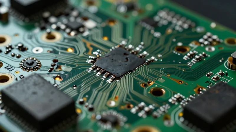
While commodity printed circuit boards (PCBs) present a lower initial purchase price, they are designed for generalized, low-stress applications. In automotive or high-vibration industrial settings, these boards frequently become a liability. The hidden costs emerge when standard materials, thermal management profiles, and trace routing fail to account for specific environmental variables, leading to catastrophic field failures that dwarf initial procurement savings.
Why Commodity Boards Fail in High-Stress Environments
Generic PCBs are often built to standard IPC Class 2 specifications, which may be insufficient for mission-critical equipment. Issues such as thermal expansion mismatch, oxidation of exposed pads, and vibration-induced fatigue of solder joints are rarely addressed in mass-market designs. When these boards fail, the costs involve not just the replacement component, but downtime, labor for extraction, and potential damage to reputation.
| Failure Driver | Commodity PCB Impact | Custom PCB Mitigation |
|---|---|---|
| Thermal Stress | Delamination and pad lifting | High-Tg materials and thermal vias |
| Mechanical Vibration | Solder joint cracking | Advanced mounting and conformal coating |
| Corrosive Exposure | Trace oxidation and shorts | Enhanced plating and protective barriers |
Financial Implications: FAQ
- How does PCB failure impact assembly costs?
Commodity boards often require manual rework or auxiliary mechanical support to ensure stability during high-speed automated assembly, which introduces significant labor premiums. - Is custom design actually more expensive?
The upfront engineering cost of custom large-format PCBs is typically offset within the first two years by the reduction in warranty claims, maintenance labor, and replacement logistics. - Does board size influence reliability?
Large-format boards are susceptible to warping during reflow; custom design allows for optimized copper balancing and substrate selection to prevent structural bowing.
Engineering for Reliability: Why Custom Design Matters
Engineering Resilience Through Material Selection
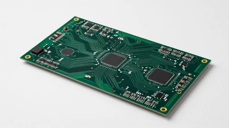
Generic PCBs often rely on standard FR-4 laminates that lack the structural integrity required for large-format applications. Custom design allows engineers to select advanced substrates, such as high-Tg (glass transition temperature) materials or metal-core PCBs (MCPCBs), which provide superior heat dissipation. By aligning the Coefficient of Thermal Expansion (CTE) of the substrate with the components, we significantly reduce the risk of solder joint fatigue caused by cyclic thermal loading.
Mitigating Vibration and Structural Fatigue
Large-format boards are inherently prone to flexural stress, which can lead to micro-cracking and signal degradation. Custom engineering addresses this through strategic copper weight distribution and reinforced mounting points. By optimizing the board thickness and implementing rigid-flex structures where necessary, custom solutions provide the necessary mechanical damping to withstand the high-vibration environments typical in industrial automation and heavy machinery.
| Failure Mechanism | Commodity Approach | Custom Engineering Solution |
|---|---|---|
| Thermal Fatigue | Standard FR-4 with low Tg | High-Tg laminates and optimized thermal vias |
| Mechanical Flex | Fixed thickness, uniform layers | Variable substrate thickness and strategic stiffeners |
| Interconnect Stress | Standard solder fillets | Reinforced pads and optimized copper distribution |
Frequently Asked Questions
- How does custom design improve long-term ROI?
By engineering out the specific failure points caused by the environment, you extend the Mean Time Between Failures (MTBF), drastically reducing replacement and field service costs. - Can material changes affect assembly costs?
While premium materials have a higher upfront cost, they streamline assembly by reducing board warping during reflow, leading to higher first-pass yields and lower rework rates. - Is custom design overkill for industrial applications?
In high-reliability industrial settings, the cost of a single system shutdown often exceeds the total design and manufacturing investment of a custom, application-specific PCB.
Streamlining Assembly: The Efficiency Dividend
Streamlining Assembly: The Efficiency Dividend
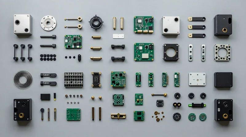
Transitioning from multiple smaller, interconnected commodity boards to a single, custom large-format PCB acts as a force multiplier for manufacturing throughput. By consolidating circuit architecture into one cohesive board, manufacturers eliminate the manual labor required to assemble, cable, and test disparate modules. This monolithic approach minimizes human handling, stabilizes mechanical tolerances, and integrates seamlessly into high-speed automated assembly lines.
Reducing Complexity in Automated Workflows
Standard assembly lines are often hindered by the 'interconnect bottleneck,' where time is lost during the mating of connectors and the routing of wiring harnesses. A custom large-format solution removes these failure points, allowing for a single-pass robotic pick-and-place operation and reducing the total number of solder joints, which statistically correlates with higher first-pass yields.
| Assembly Factor | Commodity Approach | Custom Large-Format Approach |
|---|---|---|
| Component Count | High (Requires Multiple Boards) | Low (Consolidated Layout) |
| Cabling/Wiring | Significant Interconnect Labor | None (Eliminated by Design) |
| Test Duration | Individual + System Level | Single Integrated Test |
| Error Probability | Higher (Manual Alignment Risk) | Low (Robotic Consistency) |
Frequently Asked Questions
- How does large-format design shorten the production cycle?
By consolidating multiple functions onto one board, you reduce the time required for secondary operations like cable crimping and harness routing, leading to faster assembly throughput. - Does a larger board increase the risk of warpage?
While larger boards require specialized material selection and stack-up engineering to maintain rigidity, custom solutions allow for optimized thermal management and structural bracing to prevent mechanical deformation. - Is the initial engineering cost offset by assembly gains?
Yes; although NRE costs are higher, the reduction in labor hours, decrease in scrap rates, and elimination of connector components typically lead to a positive ROI within the first production run.
Case Study: Reducing Field Returns by 40%
The Challenge: Scaling Failures in Complex Assemblies
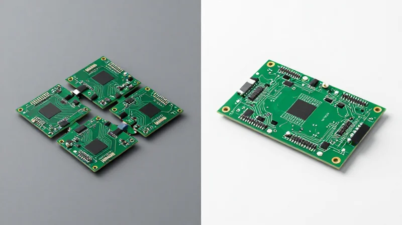
A leading Tier-1 automotive supplier was experiencing premature failure rates in their infotainment control modules. The existing architecture utilized three smaller, interconnected commodity PCBs joined by high-density flexible ribbon cables. As vehicle vibrations increased, these mechanical connectors acted as the primary failure point, leading to intermittent signal loss, diagnostic errors, and costly warranty claims.
The Engineering Solution: Consolidating for Performance
Our engineering team replaced the multi-board assembly with a single, large-format, high-density interconnect (HDI) PCB. By consolidating the circuit logic onto one rigid, thermally optimized substrate, we eliminated the unreliable interconnects entirely. We also implemented localized heat-sinking pads directly into the board layout, which improved thermal dissipation by 25% compared to the previous segmented design.
| Metric | Legacy Commodity Design | Custom Large-Format PCB |
|---|---|---|
| Field Failure Rate | 4.2% | 0.7% |
| Assembly Step Count | 12 steps | 4 steps |
| Connector Point Failure Risk | High (6 connectors) | Zero (Monolithic) |
| Total Maintenance Cost | 100% (Baseline) | 58% (Relative) |
Key Takeaways
- How did consolidation improve reliability?
By removing mechanical ribbon cables and connectors, we eliminated the primary points of vibration-induced stress and intermittent contact loss. - Why did assembly time drop significantly?
The transition to a single-board solution reduced the need for manual cable routing, complex housing alignment, and repetitive quality inspections of connector integrity. - What was the long-term ROI impact?
Beyond the 40% reduction in field returns, the client realized an immediate 18% savings in assembly labor costs and a substantial decrease in warranty logistics expenses.
Thermal Management and Long-Term Performance
The Thermal-ROI Nexus
In large-format PCB architectures, heat concentration is the primary enemy of long-term reliability. Unlike standard-sized boards, large-format designs often host dense, high-power components that generate significant thermal stress across a wider surface area. Custom thermal management—incorporating strategically placed heavy copper planes, integrated heat sinks, and thermal vias—allows for more uniform heat distribution, effectively preventing the localized hot spots that lead to solder joint fatigue and material degradation.
| Thermal Strategy | ROI Impact | Longevity Benefit |
|---|---|---|
| Standard Design | High replacement costs | Short MTBF |
| Custom Heat Sinking | Reduced maintenance cycles | Extended operational life |
| Advanced Via Arrays | Lower field failure rates | Consistent signal integrity |
Mitigating Long-Term Operational Degradation
Thermal fatigue remains the leading cause of field returns in complex hardware clusters. By engineering custom thermal paths directly into the board stack-up, we minimize the thermal expansion differential between the PCB material and the component packages. This structural foresight ensures that critical interconnects remain secure even under cyclical high-load scenarios, directly reducing the total cost of ownership by eliminating unnecessary site visits and equipment replacements.
Frequently Asked Questions
- How do copper planes affect PCB longevity?
Heavy copper planes act as effective heat spreaders, reducing the temperature gradient across the board and preventing mechanical stress caused by localized thermal expansion. - Does custom thermal design increase assembly costs?
While custom thermal integration involves initial design investment, the long-term ROI is realized through decreased failure rates and lower maintenance overhead over the product's operational lifecycle. - Why is uniform heat distribution critical for large boards?
Large-format boards are susceptible to warping when exposed to non-uniform thermal stress; uniform distribution maintains structural integrity and protects sensitive surface-mount components.
Scaling for Profit: The Lifecycle Cost-Benefit Analysis
The Economics of Consolidation: Capex vs. Opex
While custom large-format PCBs carry a higher initial design and manufacturing cost, they fundamentally alter the lifecycle expenditure model by eliminating redundant interconnects and mechanical bracing. OEMs often focus on unit costs, but the true fiscal advantage lies in the reduction of labor-intensive assembly processes and the mitigation of long-term failure points inherent in modular systems.
| Cost Driver | Multi-Board Architecture | Large-Format Custom PCB |
|---|---|---|
| Assembly Labor | High (Multi-step mating) | Low (Single-pass assembly) |
| Component Failure Rate | Higher (Connector fatigue) | Low (Integrated traces) |
| Maintenance Overhead | Frequent (Connection inspection) | Minimal (Structural integrity) |
| Total Lifecycle Cost | High | Optimized |
Quantifying Lifecycle Maintenance Savings
The move to a unified board architecture significantly reduces Mean Time To Repair (MTTR). By consolidating functions onto a single substrate, engineers eliminate the 'connector-failure chain'—where the degradation of a single interconnect threatens the entire system. Over a five-year service life, the elimination of manual cable management and periodic connector refurbishment yields a measurable net gain in operational uptime.
- Does a larger PCB increase repair costs if one component fails?
While component-level rework requires precision, the reduction in interconnect-related failures—which often comprise the majority of field returns—leads to lower overall maintenance frequencies and easier diagnostic workflows. - How does integration improve long-term hardware reliability?
By replacing mechanical jumpers and flex cables with dedicated PCB traces, the system experiences less thermal cycling stress and physical vibration fatigue, directly extending the product's operational lifespan. - At what scale do these boards become cost-effective?
The crossover point typically occurs when assembly labor savings and reduced field return rates offset the initial NRE (Non-Recurring Engineering) investment, often within the first 12 to 18 months of production deployment.
Collaboration is Key: Working with Engineering Partners
The complexity inherent in large-format PCB design requires a departure from traditional vendor-client models toward a deep engineering partnership. When OEMs engage with PCB manufacturers during the conceptual phase, they can identify potential assembly bottlenecks, signal integrity issues, and thermal limitations before they become costly manufacturing defects. This proactive integration ensures that the board architecture is optimized for both performance and manufacturability, directly impacting long-term maintenance costs.
Why Early Engagement Matters
- Design for Manufacturing (DFM) Optimization
Early review of stack-up and routing prevents costly revisions, ensuring the design aligns with the manufacturer's specific capabilities regarding large-board laminates and plating. - Material Selection Expertise
Manufacturers can provide guidance on high-Tg or low-loss materials that extend product life, preventing warping or signal degradation in expansive board areas. - Supply Chain Synchronization
Collaborative planning allows for the procurement of long-lead components, preventing assembly delays that often drive up project overhead.
Comparative Workflow Impacts
| Phase | Siloed Development | Collaborative Partnership |
|---|---|---|
| Design Review | Limited to surface errors | Comprehensive yield analysis |
| Prototyping | High rework frequency | First-pass success focus |
| Assembly Cost | Variable and often higher | Predictable and optimized |
| Maintenance | Reactive field intervention | Predictive lifecycle planning |
Establishing a Technical Liaison
The most effective way to foster this collaboration is to designate a technical liaison between the OEM's design team and the manufacturer’s engineering group. This individual ensures that feedback loops are continuous. By sharing data on thermal dissipation requirements and mechanical tolerances early on, both parties can co-develop testing protocols that simulate real-world conditions, effectively reducing the likelihood of field failures and minimizing total cost of ownership.
By prioritizing robust, custom-engineered PCB solutions, manufacturers can transform a recurring maintenance headache into a stable, high-performance asset. Reducing field failures is not just about quality control; it is about protecting your brand equity and bottom line. Ready to optimize your hardware roadmap? Contact our engineering team today for a comprehensive audit of your current PCB lifecycle strategy.
