
In the high-stakes world of automotive and industrial display integration, large-format PCBs present unique engineering hurdles. While designers often focus on functionality, the bridge between a schematic and a high-yield production run lies in rigorous Design for Manufacturing (DFM) principles. This guide explores how to optimize your layout to conquer structural instability and thermal challenges, ensuring your precision instruments perform flawlessly under pressure.
Understanding the Challenges of Large-Format PCB Assemblies
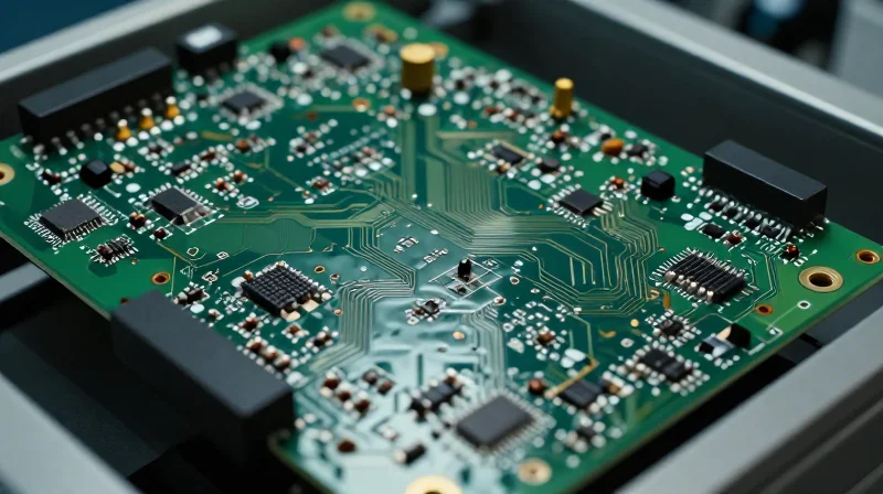
Mechanical Rigidity and Structural Integrity
Large-format boards, often exceeding 400mm in length, are inherently susceptible to warping and deflection. During the automated assembly process, the board's own weight and thermal cycling can induce mechanical stress, leading to fractured solder joints and micro-cracking in high-density interconnects. Designers must prioritize rigid mounting points and stiffener integration to maintain planarity throughout the production lifecycle.
Thermal Management at Scale
Thermal expansion coefficients (CTE) become a critical failure point when dimensions increase. Non-uniform heating during reflow can lead to 'board bowing,' where the central areas of the PCB experience different thermal profiles than the perimeter. This phenomenon risks catastrophic misalignment for fine-pitch components like BGA or LGA packages.
| Challenge | Primary Risk | DFM Mitigation |
|---|---|---|
| Board Warpage | Solder Joint Fracture | Increased PCB thickness |
| CTE Mismatch | Delamination | Symmetric layer stackup |
| Handling Stress | Trace Micro-cracking | Dedicated support fixtures |
FAQs: Navigating Large-Format PCB Assembly
- How does board size impact throughput?
Large PCBs often exceed standard conveyor widths, requiring custom-engineered handling rails and potentially slowing cycle times to allow for precise thermal distribution during reflow. - Why is layer stackup symmetry vital?
Asymmetrical copper distribution across large surface areas causes the board to bow during the curing or reflow phases as cooling rates vary between the top and bottom layers. - Can support pins prevent defects?
Yes, utilizing adjustable support pins under heavy components during the reflow process is essential to counteract gravity-induced deflection.
Mitigating Board Warpage Through Balanced Copper Distribution

The Physics of Copper-Induced Warpage
Copper and FR-4 possess vastly different Coefficients of Thermal Expansion (CTE). During the thermal cycling of reflow soldering, unbalanced copper layers act as bimetallic strips, creating internal stresses that lead to bowing and twisting. In large-format boards, these forces are magnified, making symmetrical layer stacks non-negotiable for precision instrument clusters.
Design Guidelines for Symmetry
- Maintain Stack-up Symmetry
Ensure that the copper thickness, pattern density, and foil type are matched across the neutral axis of the board. Mirroring layers (1 and N, 2 and N-1) is the primary defense against internal stress. - Implement Copper Thieving
In areas with low signal density, add non-functional copper polygons or 'thieving' to match the copper percentage of adjacent layers, ensuring uniform thermal expansion across the surface area. - Distribute Planes Evenly
Avoid stacking power and ground planes on only one side of the dielectric. Distributed planes help equalize the mechanical tension exerted on the core materials.
Copper Balancing Strategy Comparison
| Strategy | Effectiveness | Implementation Complexity |
|---|---|---|
| Symmetric Layer Stacking | High | Moderate |
| Copper Thieving (Patterns) | Medium | Low |
| Uniform Plane Pouring | High | High |
Validation Workflow
Before finalizing the Gerber data, designers should conduct a copper density analysis. Use your EDA tool to calculate the percentage of copper on each layer. A variance of more than 5% between mirror-image layers is a red flag for large-format manufacturing, as it significantly increases the risk of board deviation beyond flatness specifications required for precision instrument interfaces.
Material Selection Strategy for Large-Scale Stability
Strategic Material Selection for Thermal Stability
In large-format PCBs, dimensional stability is the cornerstone of assembly precision. When dealing with extended board areas, the differential expansion between copper features and the dielectric substrate can lead to significant latent stress. Engineers must prioritize high-Tg (glass transition temperature) laminates, typically exceeding 170°C, to prevent the material from transitioning into a rubbery, unstable state during reflow cycles. Furthermore, integrating low-CTE (Coefficient of Thermal Expansion) materials is essential to minimize Z-axis expansion, which protects sensitive via-interconnects from fatigue-induced cracking.
Laminate Property Comparison
| Material Class | Typical Tg (°C) | CTE (ppm/°C) | Application Focus |
|---|---|---|---|
| Standard FR-4 | 130-140 | 15-18 | General Purpose/Consumer |
| High-Tg FR-4 | 170-180 | 12-14 | Automotive/Precision Clusters |
| Advanced Ceramic-Filled | 200+ | 9-11 | Extreme Thermal/High-Speed |
Material Selection FAQ
- Why is Tg critical for large-format boards?
A higher Tg ensures the resin matrix remains rigid throughout the entire thermal processing window, preventing excessive board softening and subsequent warpage that occurs as board size increases. - Does low-CTE always imply higher cost?
Generally, yes. Materials with specialized fillers designed to match copper's CTE are more expensive, but they significantly reduce the total cost of ownership by eliminating yield losses associated with cracked vias and registration errors. - Can I mix laminate types on one board?
Mixing materials is strongly discouraged for large-format designs. Differences in material properties lead to asymmetric tension, drastically increasing the likelihood of catastrophic bow and twist during assembly.
Advanced Routing Techniques for High-Speed Signal Integrity

Precision Impedance Control at Scale
Maintaining consistent characteristic impedance across large-format panels is hindered by laminate thickness tolerances and copper etching variations. For high-speed signal paths, engineers must employ differential pair routing with strict length matching and minimize layer transitions to prevent reflections. Utilizing laser-drilled microvias can significantly reduce via-stub capacitance, which is critical for signal frequencies exceeding 5GHz.
| Strategy | Benefit | Design Consideration |
|---|---|---|
| Back-drilling | Eliminates via stubs | Adds manufacturing cost |
| Zig-zag Routing | Adjusts path length | Must avoid sharp angles |
| Ground Stitching | Reduces EMI loop area | Requires consistent spacing |
Routing Best Practices
- How do you manage impedance variance?
Apply target impedance calculations early, accounting for etch factor compensation provided by the fabricator to ensure the actual width matches the design intent. - Is layer transition routing recommended?
Avoid crossing reference plane discontinuities. If a transition is necessary, place stitching vias immediately adjacent to the signal via to maintain a continuous return current path. - How to handle high-speed signal crosstalk?
Increase inter-pair spacing to at least 3x the dielectric height and implement guard traces connected to ground for critical, long-run signals.
Automation and DFM Analysis
For large boards, manual routing is prone to inconsistency. Use automated length-tuning scripts within your CAD environment to ensure phase matching. Furthermore, perform post-layout SI (Signal Integrity) simulation to verify eye diagrams against industry standards like PCIe or LVDS requirements, ensuring the design is resilient to manufacturing tolerances.
Optimizing Panelization and Fiducial Placement

Strategic Panelization for Material Efficiency
In large-format manufacturing, maximizing panel utilization is not merely a cost-saving measure but a structural necessity. Aligning board orientation with the grain of the laminate material is critical for minimizing residual stress and subsequent warpage during reflow. Designers should prioritize nested arrays that balance the copper distribution across the entire panel area, effectively neutralizing the mechanical tension created during the lamination process.
| Parameter | Best Practice | Impact |
|---|---|---|
| Array Margin | Minimum 10mm | Improved mechanical stability |
| Board Spacing | 2.5mm to 5mm | Easier depaneling/routing |
| Copper Balance | >70% uniformity | Prevents board bowing |
Fiducial Mark Precision and Placement
For large-format instrument clusters, fiducial placement requires a hierarchical approach to support global and local alignment. Camera-based optical recognition systems rely on high-contrast markers to calculate precise coordinates; insufficient or poorly placed fiducials frequently result in placement errors, particularly on the edges of large boards where thermal expansion is most pronounced.
- How many fiducials are required?
A minimum of three fiducials is mandatory for global alignment, placed in a non-symmetrical pattern to allow the software to identify the board orientation. For large-format panels, add secondary fiducials near fine-pitch components (local fiducials) to compensate for localized thermal expansion. - What are the design requirements for fiducial marks?
Marks must be solid copper pads, ideally circular, with a diameter of 1mm and a clear solder mask keep-out zone at least 2mm around the perimeter to ensure high-contrast image processing. - Why do large panels require edge fiducials?
Edges of large-format boards undergo the most significant CTE-induced movement. Placing fiducials near the corners of the panel allows the pick-and-place equipment to perform a global coordinate shift based on real-time board geometry.
Thermal Management at Scale

Engineered Heat Dissipation Strategies
In high-brightness display applications, thermal density is the primary enemy of long-term reliability. For large-format PCBs, traditional heat sinking is often insufficient due to the expansive surface area and mechanical constraints. Instead, designers must utilize the copper stack-up itself as a primary thermal conduit. This requires increasing copper weight in inner layers—typically 2oz or greater—to create low-resistance paths for heat transition from active driver ICs to the board substrate.
| Technique | Primary Function | Implementation Tip |
|---|---|---|
| Copper Pours | Lateral heat spreading | Flood unused board areas with ground-tied copper. |
| Thermal Vias | Vertical heat transfer | Use a 0.2mm to 0.3mm diameter grid for optimal flux. |
| Heat Sinking Mids | Interface management | Directly bond driver thermal pads to internal planes. |
Strategic Thermal Via Design
Thermal vias must be placed with precision to avoid disrupting impedance-controlled traces while maximizing thermal dissipation. For large-format panels, stitching vias into an array directly under the thermal pad of high-brightness drivers is essential. It is recommended to use non-conductive filled and capped vias (VIPPO) to prevent solder wicking and ensure a flat surface for reliable thermal coupling between the IC and the PCB.
- How does PCB thickness impact thermal dissipation?
Thicker boards provide higher thermal mass but require more robust via designs to move heat from the top layer to the internal heatsinking planes. - Why is copper weight critical for display drivers?
Higher copper weights reduce electrical resistance and lower the thermal resistivity of the board, allowing heat to spread laterally away from concentrated hotspots. - Can I use external heat sinks on large formats?
Yes, but they must be carefully matched to the CTE of the PCB material to prevent mechanical warping during thermal cycling.
Establishing a Collaborative DFM Workflow with Your Manufacturer
The complexity of large-format PCB manufacturing necessitates a shift from a reactive to a collaborative Design for Manufacturing (DFM) methodology. By engaging with your manufacturer during the conceptual phase, you can identify potential fabrication bottlenecks—such as panel distortion, registration tolerances, or material selection—long before the design is committed to high-volume production.
Synchronizing Data and Communication
The cornerstone of a successful DFM workflow is the exchange of unified, machine-readable design data. Relying on outdated or proprietary formats often leads to misinterpretations that manifest as defects in the final assembly. Establishing a shared data protocol ensures transparency regarding stack-up requirements, impedance constraints, and critical tolerances.
| Collaborative Element | Legacy Approach | Modern DFM Workflow |
|---|---|---|
| Communication Timing | Post-layout review | Pre-layout design consultation |
| Data Exchange | Static Gerber files | ODB++ or IPC-2581 containers |
| Tolerance Feedback | Manual email cycles | Integrated DFM analysis tools |
Frequently Asked Questions: Establishing DFM Partnerships
- Why is early-stage engagement critical for large-format PCBs?
Large boards are susceptible to thermal expansion and warping during lamination; early engagement allows the manufacturer to optimize stack-up and copper distribution to mitigate these risks. - What data formats should be standardized for collaboration?
Utilizing intelligent formats like ODB++ or IPC-2581 is vital because they embed component data, stack-up information, and netlist integrity into a single file structure, reducing the chance of manual parsing errors. - How do I balance design goals with manufacturer constraints?
Maintain a 'Design Rule Document' shared in real-time with the fabricator to ensure that design targets for trace width and clearance remain within the factory’s current process capability (CpK).
Achieving high yields in large-format PCB manufacturing is not a matter of luck; it is the result of disciplined DFM integration and proactive material planning. By addressing warpage, copper balancing, and layout complexity upfront, you minimize costly re-spins and ensure market-ready product performance. Ready to optimize your next design? Contact our engineering team today for a comprehensive DFM audit of your project.
