
The rapid expansion of electric vehicle infrastructure demands hardware that can withstand extreme electrical loads without compromising safety. As charging stations shift toward faster, higher-power outputs, the printed circuit board (PCB) becomes the critical bottleneck. Selecting the right heavy copper PCB is no longer just about current—it is about thermal efficiency, long-term reliability, and precise engineering. This guide breaks down the essential factors for engineers and project managers looking to future-proof their EV charging designs.
Understanding the Role of Heavy Copper in Power Electronics
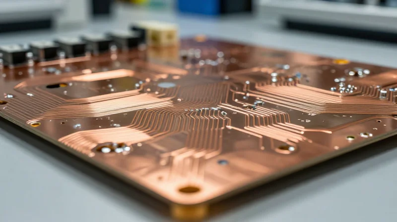
Why Heavy Copper is Mandatory for EV Infrastructure
In high-power EV charging systems, power modules must handle continuous high-current loads—often reaching hundreds of amperes. Standard PCB copper weights are insufficient for these demands, leading to excessive voltage drops and catastrophic thermal failure. Heavy copper, typically defined as 3oz per square foot or greater, effectively reduces DC resistance, allowing for efficient power transmission while minimizing power dissipation in the form of heat.
Core Benefits of High-Copper Integration
- Thermal Management
Increased cross-sectional area allows copper traces to act as effective heatsinks, distributing thermal load across the PCB and preventing localized hotspots. - Reduced Voltage Drop
Lower resistance minimizes power loss, ensuring that maximum voltage is delivered to the load, which is critical for maintaining charging efficiency in long-duration cycles. - Mechanical Robustness
Heavy copper layers provide superior mechanical strength, better tolerating high-current pulses and potential thermal expansion stresses associated with repetitive charging cycles.
Performance Comparison: Standard vs. Heavy Copper
| Feature | Standard PCB (1oz) | Heavy Copper (3oz+) |
|---|---|---|
| Current Capacity | Low (Limited) | High (Excellent) |
| Thermal Dissipation | Poor | Superior |
| Power Efficiency | Reduced by I2R loss | High (Minimal I2R) |
| Target Application | Consumer Electronics | EV/Industrial Power |
Calculating Current-Carrying Capacity and Trace Widths
Applying IPC Standards for Thermal Management
To prevent catastrophic failure in EV charging modules, design engineers must move beyond simple DC resistance calculations and utilize established IPC standards. IPC-2221, the legacy standard, provides conservative design guidelines, while IPC-2152 represents the modern benchmark, offering a more nuanced, empirical approach to internal and external layer temperature rise predictions.
| Standard | Methodology | Best Use Case |
|---|---|---|
| IPC-2221 | Simplified, conservative empirical curves | Initial prototyping and non-critical layouts |
| IPC-2152 | Comprehensive, physics-based thermal modeling | High-power EV charging, high-density power stages |
Key Factors for Trace Calculation
When calculating trace dimensions for heavy copper applications, the following variables must be balanced to maintain an acceptable temperature rise (typically 10°C to 20°C for power electronics):
- Current Magnitude
The steady-state and peak current load determines the required cross-sectional area of the copper trace. - Allowable Temperature Rise
Engineers must define the maximum permitted temperature delta above ambient to ensure dielectric material integrity. - Layer Placement
Internal layers dissipate heat significantly slower than external layers, necessitating wider traces for the same current load.
Common Implementation Questions
- Why is IPC-2152 preferred over IPC-2221 for high-power EV systems?
IPC-2152 accounts for a wider variety of board geometries and thermal environments, reducing the risk of over-engineering or, more dangerously, under-estimating thermal bottlenecks. - How does heavy copper affect manufacturing tolerances?
Increased thickness alters the etch factor during PCB fabrication; designers must coordinate with their fabricator to ensure the final etched width matches the calculated design requirements.
Evaluating Substrate Materials for High-Power Stability
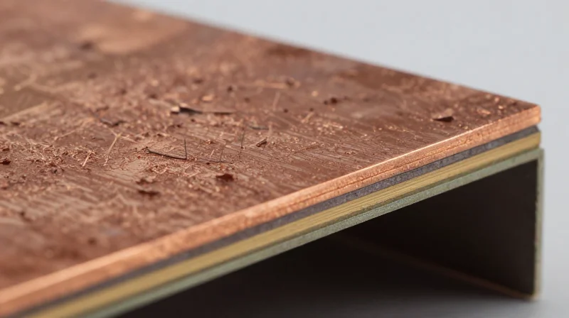
When heavy copper PCBs carry high currents, the resulting heat generation poses significant challenges to standard dielectric materials. Selecting the correct substrate involves balancing thermal conductivity, glass transition temperature (Tg), and the Coefficient of Thermal Expansion (CTE) to prevent mechanical failure during the rapid thermal cycling typical of EV charging infrastructure.
Comparative Analysis of Substrate Materials
| Material Type | Thermal Conductivity (W/mK) | Tg (°C) | Best Use Case |
|---|---|---|---|
| Standard FR-4 | 0.25 | 130-140 | Low-power control logic |
| High-Tg FR-4 | 0.3 - 0.4 | 170-180 | High-power industrial chargers |
| Ceramic-Filled Laminate | 1.0 - 3.0+ | >200 | Extreme power density/Fast charging |
Key Considerations for Thermal Stability
- Why is Tg significant for heavy copper PCBs?
A high glass transition temperature (Tg) ensures the board material remains rigid and avoids excessive expansion when operating near peak thermal limits, protecting the integrity of heavy copper vias. - When should ceramic-filled laminates be selected?
Ceramic-filled laminates are required when power density is so high that standard resin-based substrates would degrade due to poor heat dissipation, even with heavy copper. - How does CTE mismatch impact reliability?
Heavy copper and substrate materials expand at different rates; selecting a material with a low and stable CTE prevents copper delamination and interconnect fractures under repeated thermal cycling.
For EV charging infrastructure, we recommend prioritizing high-Tg laminates as a baseline. Ceramic-filled substrates should be reserved for power modules where localized heat density threatens to exceed the dielectric threshold, ensuring long-term operational lifespan in demanding outdoor environments.
Thermal Management Strategies for Dense PCB Layouts
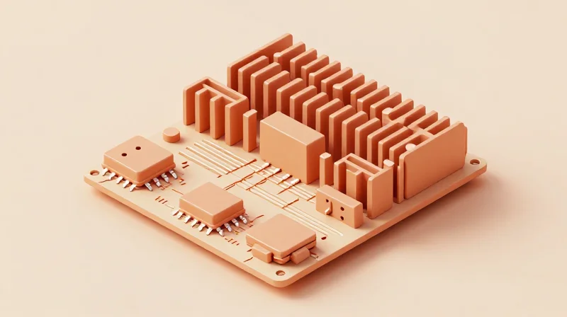
Advanced Thermal Dissipation Techniques
In high-power EV charging modules, copper thickness alone is insufficient to prevent localized hotspots. Engineers must leverage thermal management as a primary design constraint, prioritizing low-impedance heat paths that bridge the gap between high-power MOSFETs and the external chassis or heatsink.
Thermal Vias and Copper Pour Strategy
Thermal vias act as vertical heat pipes. For optimal performance, utilize a tightly packed array of copper-plated through-holes directly beneath the power component's thermal pad. It is critical to fill and cap these vias (VIPPO) to prevent solder wicking while maximizing copper volume for vertical heat transfer.
| Strategy | Primary Benefit | Design Consideration |
|---|---|---|
| Thermal Vias | Z-axis heat transfer | Ensure plating thickness is >= 25um |
| Copper Pour | Increased surface area | Avoid thermal relief on high-current pads |
| Heat Sinks | Convective dissipation | Requires high-k thermal interface material |
Frequently Asked Questions on Thermal Design
- How does heavy copper affect thermal relief patterns?
For high-current connections, standard thermal reliefs can act as current bottlenecks. Use solid copper connections to the plane to reduce resistance and facilitate maximum heat spreading. - Should I use aluminum or copper-backed PCBs?
While aluminum-backed boards offer excellent thermal conductivity, heavy copper FR-4 boards are often preferred for EV charging due to superior mechanical stability and standard multilayer routing capabilities. - What is the impact of solder mask on heat dissipation?
Solder mask acts as an insulator. For critical thermal pads, consider exposing the copper and applying a direct finish like ENIG or Immersion Silver for better contact with thermal interface materials.
The Impact of Plating Quality on Reliability
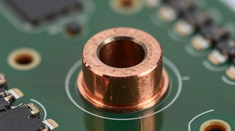
The Critical Role of Through-Hole Plating Uniformity
In heavy copper PCB applications for EV charging stations, the barrel plating in plated through-holes (PTH) is the most common point of mechanical failure. Because high-power charging involves significant thermal cycling—rapid transitions between ambient temperatures and high operating heat—any non-uniformity in copper plating thickness introduces stress concentrations. When the thermal expansion coefficient (CTE) mismatch between the copper barrel and the surrounding laminate is poorly managed due to thin or inconsistent plating, the resulting hoop stress can cause barrel cracking or pad lifting, leading to intermittent signal loss or catastrophic electrical failure.
Plating Quality vs. Thermal Reliability Metrics
| Failure Mechanism | Impact of Poor Plating | Mitigation Strategy |
|---|---|---|
| Barrel Cracking | High stress during thermal cycling leading to open circuits. | Ensure minimum 25µm average plating thickness in holes. |
| Pad Lifting | Loss of electrical connection due to board delamination. | Optimize drilling parameters and utilize high-Tg laminates. |
| Current Crowding | Hot spots in corners caused by thin copper distribution. | Use pulse-periodic reverse plating for uniform distribution. |
Common Concerns Regarding Plating Resilience
- How does aspect ratio affect plating quality?
Higher aspect ratio holes make it difficult for plating solutions to reach the center of the barrel, often resulting in thinner copper in the middle compared to the entry/exit points. For heavy copper, keeping aspect ratios low is vital for structural integrity. - Why is surface finish choice relevant to plating durability?
While HASL provides a robust coating, the thermal shock of the process can stress the hole walls. For high-reliability EV systems, ENIG or Immersion Silver are often preferred to ensure a flatter, more uniform surface that doesn't put additional mechanical strain on the PTH. - Can non-uniform plating be detected before installation?
Yes, micro-section analysis is the industry standard. By cutting through the finished PCB and examining the cross-section under magnification, engineers can measure the exact copper thickness in the hole walls to verify compliance with IPC Class 3 standards.
Surface Finishes and Their Influence on Power Handling
In high-power EV charging modules, the surface finish acts as the final interface between the massive copper traces and critical power components. Choosing a finish that facilitates low-resistance interconnects while preventing oxidation is essential, as the high current densities found in these systems can rapidly accelerate thermal degradation if the junction interface is compromised.
Evaluating Surface Finish Performance for High-Current Applications
| Finish Type | Conductivity Impact | Thermal Reliability | Best Use Case |
|---|---|---|---|
| ENIG | Moderate | Good | High-density signal pins |
| Immersion Silver | High | Moderate | Power stage connections |
| ENEPIG | High | Excellent | High-reliability power modules |
| OSP | Excellent | Low | Cost-sensitive power boards |
Common Considerations for Heavy Copper Finishes
- Why is immersion silver favored for high power?
Immersion silver provides a highly conductive, planar surface that is ideal for large-pad components, ensuring maximum contact area for heavy-duty power MOSFETs and diodes. - Is ENIG suitable for power-heavy charging hardware?
While ENIG is excellent for fine-pitch surface mount components, its nickel layer can introduce higher contact resistance compared to silver-based finishes, which may be a concern in extremely high-amperage paths. - How does surface flatness affect power delivery?
In EV charging infrastructure, uneven surface finishes can lead to localized hotspots at solder joints due to inconsistent wetting, whereas a planar finish ensures uniform current distribution across the entire contact pad.
For long-term reliability in EV charging environments, ENEPIG (Electroless Nickel Electroless Palladium Immersion Gold) is increasingly preferred. By incorporating a palladium barrier layer, it effectively prevents nickel corrosion and allows for multiple reflow cycles, providing the robust mechanical and electrical foundation required for continuous 24/7 operation under thermal load.
Safety Standards and Regulatory Compliance
For EV charging infrastructure, heavy copper PCBs are subject to rigorous safety standards because they facilitate the transmission of high-voltage, high-current electricity. Failure to comply with international regulations such as UL 796 and various IEC standards can lead to catastrophic hardware failure, fire hazards, or operator injury. Designers must prioritize dielectric integrity and spatial isolation to ensure long-term reliability in the field.
Key Regulatory Frameworks
| Standard | Focus Area | Relevance to EV Charging |
|---|---|---|
| UL 796 | PCB Construction | Mandates safety testing for base materials and copper weights. |
| IEC 60664-1 | Insulation Coordination | Defines clearance and creepage requirements for low-voltage equipment. |
| UL 94 | Flammability | Requires V-0 rating for substrates used in high-power energy management. |
Critical Design Factors: Creepage and Clearance
Creepage and clearance are the primary defense against electrical arcing. Clearance is the shortest path between two conductive parts through the air, while creepage is the shortest path along the surface of the insulating material. In heavy copper designs, where voltage gradients are significant, insufficient spacing leads to potential dielectric breakdown, especially in humid or dusty charging environments.
Regulatory Compliance FAQ
- How does heavy copper thickness influence creepage requirements?
Increased copper thickness can lead to lateral protrusions after etching; these protrusions may reduce effective creepage distances, requiring more aggressive design margins than standard 1oz copper. - What is the role of the Comparative Tracking Index (CTI)?
The CTI measures the insulating material's resistance to carbon tracking. Higher CTI values allow for tighter board spacing, which is critical when miniaturizing EV charging control circuitry. - Are there specific requirements for conformal coating?
Yes, high-power PCB assemblies often require conformal coating to meet pollution degree requirements (PD2 or PD3), effectively improving the board's environmental rating without increasing physical trace spacing.
Selecting the Right Manufacturing Partner
Critical Evaluation Criteria for Heavy Copper Fabricators
Not every PCB manufacturer is equipped to handle the unique thermal and structural demands of heavy copper (2oz to 20oz+). When selecting a partner for EV charging infrastructure, you must prioritize fabricators with proven expertise in high-current density design and deep-hole plating capabilities.
| Vetting Category | Key Requirement | Why It Matters |
|---|---|---|
| Copper Processing | Advanced Plating Uniformity | Ensures consistent current distribution and avoids localized hot spots. |
| Thermal Management | High-Tg Material Handling | Maintains structural integrity under sustained high-power charging cycles. |
| Compliance | UL/IEC Certification | Mandatory for grid-connected high-voltage EV infrastructure. |
| Process Control | Automated Optical Inspection | Detects minute defects in heavy-trace geometry that cause failure. |
Technical Auditing and Quality Assurance
Beyond surface-level credentials, demand evidence of internal process controls. A qualified partner will provide cross-sectional analysis reports confirming that copper wall thickness in plated through-holes meets your specific current-carrying requirements, regardless of the board's outer layer weight.
- Does the manufacturer have in-house capabilities for multi-stage heavy copper etching?
Outsourcing the etching process for heavy copper increases the risk of undercutting or poor side-wall profiles, which compromises the reliability of high-power traces. - Can they document their experience with high-current testing?
Ask for case studies or test data demonstrating how their PCB stacks handle thermal expansion and peak load demands common in EV charging stations. - Is the facility certified to the latest automotive and industrial standards?
Look for IATF 16949 or ISO 9001 certifications to ensure the manufacturing environment meets the rigorous quality management systems required by the automotive supply chain.
Prioritize transparency in the manufacturing flow. A partner who invites you to review their DFM (Design for Manufacturing) guidelines and allows early-stage design consultation will significantly reduce the risk of board failure in the field.
Selecting the appropriate heavy copper PCB is a defining factor in the success and safety of your EV charging infrastructure project. By balancing copper weight, substrate material, and thermal management, you can ensure your systems handle high-power demands with unwavering reliability. Are you ready to optimize your power electronics design? Contact our engineering team today to discuss your next high-performance PCB project.
