
As the demand for high-speed EV charging grows, the bottleneck isn't just the grid—it's the hardware's thermal threshold. Many network operators face soaring maintenance costs due to traditional thermal management failures in high-current applications. This guide explores how shifting to heavy copper PCB integration offers a superior, high-efficiency path to scaling your charging infrastructure while optimizing ROI.
The Thermal Challenge in Modern Fast Charging
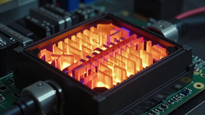
The Thermal Limitations of Standard PCBs
In the context of modern fast-charging stations, high-amperage current creates significant thermal stress on power electronics. Standard FR-4 printed circuit boards (PCBs) typically utilize 1-ounce or 2-ounce copper layers, which are sufficient for signal processing or low-power consumer electronics but insufficient for the massive energy throughput required by modern EV charging modules. When current flows through these thin traces, high resistance leads to I²R heating, resulting in rapid temperature spikes that degrade dielectric materials, lead to board warping, and ultimately trigger thermal shutdowns to prevent catastrophic component failure.
Comparative Analysis: Standard vs. Heavy Copper
| Feature | Standard PCB (1-2 oz) | Heavy Copper PCB (4+ oz) |
|---|---|---|
| Current Capacity | Low/Moderate | Extremely High |
| Thermal Dissipation | Poor | Excellent |
| Board Longevity | Limited under stress | High durability |
| Failure Risk | Elevated | Minimized |
Thermal Dynamics and Scalability Issues
To achieve faster charging times, stations must increase power output, which necessitates higher currents flowing through the power distribution stages. Without heavy copper, engineers are forced to use additional heatsinks, complex active cooling fans, or oversized components to compensate for the inability of the board to manage heat. These workarounds increase the physical footprint of the charging station, complicate assembly, and inevitably degrade the long-term Return on Investment (ROI) by introducing more points of failure and increasing maintenance costs.
Key Thermal Challenges FAQ
- Why does heat cause component degradation?
Excessive heat causes the substrate material in standard PCBs to delaminate and degrades the solder joints, eventually leading to intermittent connectivity or total board failure under high-amperage load. - Can passive cooling replace heavy copper?
Passive cooling via external heat sinks adds bulk and weight, which hampers the scalability and compact design required for modern modular charging stations. - How does heavy copper affect board resistance?
Increasing the copper cross-sectional area significantly reduces electrical resistance, allowing for higher current flow with lower heat generation, which directly preserves the integrity of the power delivery system.
What is Heavy Copper PCB Technology?
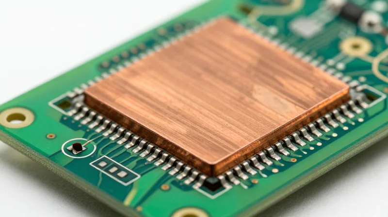
Defining Heavy Copper Technology
Heavy copper PCB technology refers to circuit boards manufactured with copper weights typically ranging from 3 ounces (oz) per square foot up to 20 oz or more, compared to the standard 0.5 oz to 1 oz found in consumer electronics. This increased metal thickness creates a significantly lower electrical resistance across the conductive paths, which is the foundational requirement for supporting the high-amperage demands of modern EV charging stations.
Engineering for Current Density
In fast-charging systems, power modules must continuously deliver hundreds of amperes to the vehicle battery. Standard PCBs would suffer from extreme ohmic heating, leading to substrate degradation and catastrophic failure. By increasing the cross-sectional area of the copper traces, heavy copper technology allows for higher current density while maintaining lower operating temperatures, effectively transforming the PCB into a structural part of the thermal management system.
| Feature | Standard PCB | Heavy Copper PCB |
|---|---|---|
| Copper Weight | 0.5 - 1.0 oz | 3.0 - 20.0+ oz |
| Heat Dissipation | Low/Moderate | High/Superior |
| Current Load | Low | Very High |
| Component Stress | High (Thermal) | Low (Thermal) |
Frequently Asked Questions
- How does extra copper assist with cooling?
The copper acts as a heat sink, spreading thermal energy away from high-power components like MOSFETs and IGBTs into the PCB laminate and out through the chassis, reducing reliance on bulky external heat sinks. - Does heavy copper impact assembly?
Yes, it requires specific fabrication adjustments including modified etching processes and specialized solder mask applications to handle the greater thickness of the copper features. - Why is this essential for ROI?
By extending the lifespan of power modules and minimizing cooling failures, heavy copper PCBs reduce maintenance costs and operational downtime, directly improving the long-term ROI of EV charging infrastructure.
Reducing Energy Loss Through Lower Resistance
The primary barrier to high-efficiency EV charging is the Joule effect, where standard copper traces act as resistive elements, converting electricity into heat rather than delivering it to the vehicle. Heavy copper PCBs (typically 3oz to 10oz copper or higher) significantly lower the DC resistance of the power path, directly minimizing power dissipation. This reduction in heat loss not only improves energy throughput but also extends the operational lifespan of the charging station by alleviating the thermal stress on delicate electronic components.
Quantifying Efficiency Gains
| Copper Weight | Resistance per Unit Length | Estimated Heat Dissipation | Thermal Management Load |
|---|---|---|---|
| 1oz (Standard) | High | Significant | Heavy/Active |
| 3oz | Moderate | Reduced | Moderate/Passive |
| 6oz+ | Very Low | Minimal | Minimal |
Addressing Thermal Impedance
Lowering resistance through thicker copper is not solely about throughput; it is about reducing thermal impedance. When resistance is lowered, the 'heat bucket' of the PCB does not fill up as quickly, which reduces the dependency on external cooling systems like high-velocity fans or liquid chillers. This leads to a dual ROI: higher energy efficiency due to less power lost as heat, and lower operational costs (OPEX) due to reduced auxiliary cooling power requirements.
Common Questions on Resistance Reduction
- Does thicker copper always guarantee better performance?
While thicker copper reduces resistance, it must be balanced with PCB manufacturing capabilities and trace spacing requirements to prevent short circuits and maintain signal integrity. - How does reduced resistance impact charging speed?
Reduced resistance lowers voltage drop across the PCB, ensuring the system can deliver a steady, high-amperage current to the EV battery, minimizing the throttling often triggered by thermal protection limits. - Can heavy copper eliminate the need for active cooling?
It significantly reduces the demand on active cooling, allowing systems to run cooler or stay at maximum charge capacity for longer durations before needing to throttle power.
Comparing Thermal Management Solutions
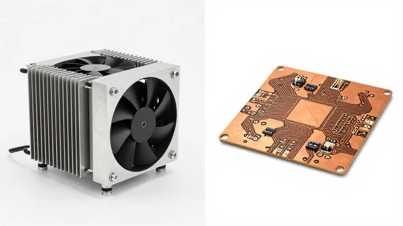
Thermal Management Strategy Comparison
Selecting the optimal thermal management solution is critical for balancing the upfront capital expenditure of an EV charging station against the long-term operational costs and equipment longevity. While traditional methods like active cooling rely on external mechanical components, heavy copper PCBs utilize integrated thermal conduction to manage high-current density directly at the circuit board level.
| Solution | Failure Risk | Energy Draw | Maintenance Requirement |
|---|---|---|---|
| Heavy Copper PCBs | Negligible (Passive) | None (Passive) | Minimal |
| Heat Sinks | Low (Dust Accumulation) | None (Passive) | Periodic Cleaning |
| Active Fans | High (Mechanical Wear) | Moderate/Continuous | Regular Replacement |
Reliability and Operational Efficiency Analysis
The primary advantage of heavy copper technology is its passive nature. By eliminating reliance on moving parts, station operators significantly reduce the mean time between failures (MTBF). Conversely, systems heavily reliant on active fan cooling introduce mechanical points of failure that increase the probability of downtime in harsh, outdoor charging environments. Furthermore, active systems consume auxiliary power to drive cooling mechanisms, which directly impacts the net energy efficiency of the charging station.
- Does heavy copper increase energy consumption?
No; heavy copper reduces ohmic heating within the PCB, thereby increasing efficiency and reducing the energy wasted as heat, unlike fans which require continuous power. - How does mechanical failure impact ROI?
Mechanical failures in cooling fans lead to unscheduled site maintenance and potential system thermal shutdowns, which directly erode ROI through lost charging revenue and service costs. - Can passive cooling replace all active cooling?
In many modern high-amperage applications, heavy copper allows for a drastic downsizing of active components, extending the life of remaining hardware and simplifying the thermal design footprint.
Impact on Long-Term Reliability and Maintenance
Thermal Mitigation as a Reliability Driver
Electronic hardware failure in high-power environments is overwhelmingly driven by thermal fatigue. Traditional PCBs often struggle with the sustained high current levels required for fast DC charging, leading to repeated expansion and contraction cycles that compromise solder joints and board substrates. Heavy copper technology acts as a primary heat-dissipation medium, effectively conducting heat away from power components and distributing it across the board surface to prevent localized hot spots. By maintaining lower operating temperatures, heavy copper PCBs preserve the dielectric integrity of the board and extend the MTBF (Mean Time Between Failures) of connected power electronics, such as MOSFETs and capacitors.
Maintenance Impact and Technician Call-outs
The reliance on mechanical cooling solutions like active fans or complex heat sinks introduces additional points of failure into charging station hardware. Each moving part or secondary cooling assembly represents a component that will eventually require inspection, cleaning, or replacement. By utilizing heavy copper to achieve superior passive cooling, operators can shift away from these high-maintenance active systems. This architectural shift significantly decreases the frequency of emergency technician call-outs, ensuring charging stations remain operational with minimal downtime.
| Reliability Metric | Standard PCB System | Heavy Copper PCB System |
|---|---|---|
| Thermal Stress | High (Frequent cycling) | Low (Stable dissipation) |
| Component Lifespan | Shortened due to heat | Extended via cooler operation |
| Maintenance Requirement | High (Fan/Filter maintenance) | Low (Passive reliability) |
| Failure Mode Risk | Solder fracture/Delamination | Minimal wear |
Frequently Asked Questions
- How does heavy copper reduce the need for field repairs?
By lowering the operating temperature of the PCB, heavy copper prevents the thermal degradation of critical components and prevents the board from warping or cracking over thousands of charging cycles. - Can I eliminate fans entirely with heavy copper?
In many high-power applications, heavy copper allows for a significant reduction in the size and speed of active cooling systems, and in some designs, it may eliminate the need for active cooling altogether, depending on the ambient environmental constraints. - Is the initial cost of heavy copper justified by maintenance savings?
Yes. While the manufacturing cost of heavy copper is higher, the ROI is realized through the drastic reduction in unscheduled maintenance, fewer replacement parts, and the mitigation of revenue loss caused by station downtime.
Calculating the Total Cost of Ownership (TCO)
The Economics of Heavy Copper Integration
Calculating TCO for high-power EV charging infrastructure necessitates a shift from focus on initial component procurement to a comprehensive evaluation of operational lifecycle costs. Heavy copper PCBs, while possessing a higher initial manufacturing cost, fundamentally alter the TCO profile by slashing energy waste and extending the MTBF (Mean Time Between Failures) of critical power modules.
| Cost Factor | Standard PCB System | Heavy Copper PCB System |
|---|---|---|
| Initial Procurement | Low | Higher |
| Energy Efficiency (I2R Loss) | High Waste | Low Waste |
| Active Cooling Costs | High (Fans/Maintenance) | Minimal (Passive) |
| Long-term Maintenance | Frequent Replacement | Extended Lifespan |
Quantifying Lifecycle Savings
To accurately model the ROI, stakeholders must quantify the reduction in energy expenditure. By lowering trace resistance, heavy copper boards reduce the heat generated during power conversion. This efficiency minimizes the energy consumed by internal cooling fans and prevents thermal throttling, which can significantly decrease the charging delivery rate at peak temperatures. Over a five-year deployment, the savings from reduced energy consumption and lower cooling infrastructure requirements often recoup the initial premium paid for heavy copper designs within the first 18 months.
Frequently Asked Questions on TCO
- Does heavy copper impact installation labor costs?
No, while the PCB itself is more robust, it fits into standard assembly processes, ensuring no additional specialized labor costs are introduced during manufacturing. - How does reduced thermal stress impact maintenance budgets?
Reduced heat leads to slower degradation of board components and solder joints, significantly reducing the frequency of on-site technician visits and module replacements. - Is the TCO benefit visible at low-power charging levels?
The ROI benefits are most pronounced in DC fast-charging applications (150kW+), where high current density makes thermal efficiency a major driver of operational cost.
Scalability and Future-Proofing Infrastructure
Designing for Modular Power Scaling
Heavy copper PCBs serve as the thermal and electrical backbone for EV charging stations, allowing designers to accommodate higher kilowatt outputs through simple software or peripheral upgrades rather than complete hardware overhauls. By utilizing thicker copper traces, these boards minimize the need for redesigning power paths when moving from standard to ultra-fast charging architectures.
Lifecycle Comparison: Heavy Copper vs. Standard PCBs
| Feature | Standard PCB (1 oz) | Heavy Copper (3oz+) | Impact on Scalability |
|---|---|---|---|
| Current Handling | Limited | Excellent | Higher capacity overhead |
| Thermal Stress | High (requires cooling) | Low (passive dissipation) | Longer component life |
| Upgrade Potential | Replacement required | In-place capacity growth | Reduces CAPEX spikes |
Strategic Benefits for Infrastructure ROI
Investing in heavy copper technology ensures that your initial installation remains relevant as EV battery technologies demand faster charging cycles. This approach eliminates the 'rip-and-replace' cycle, ensuring that site operators only need to upgrade power modules while keeping the internal bus architecture intact.
Frequently Asked Questions
- Does heavy copper increase upfront costs?
While the material cost is slightly higher than standard boards, the reduced need for thermal management hardware and future-proofing capability significantly improves ROI. - Can I upgrade from standard to heavy copper later?
Replacing a PCB after installation involves significant labor and downtime costs; it is far more efficient to integrate heavy copper at the design phase. - Does this impact global energy compliance?
Yes, by reducing resistance and heat, heavy copper improves total system efficiency, making it easier to meet stringent energy certification standards for future charging equipment.
Best Practices for Implementation
Optimizing Design for High-Current Density
The successful deployment of heavy copper circuits—defined typically as 3 oz to 10+ oz copper weights—requires moving beyond standard PCB design rules. Engineers must prioritize trace width and spacing to prevent dielectric breakdown and manage the increased etching lateral spread, which can affect impedance control.
Procurement Checklist for Heavy Copper Specification
- Thermal Via Strategy
Ensure designs incorporate an optimized array of thermal vias to dissipate heat directly into the chassis or heat sink, preventing localized hotspot formation near high-power MOSFETs. - Etch Factor Management
Specify tighter tolerances on trace sidewalls, as heavy copper processes inherently involve greater undercutting compared to standard 1 oz copper boards. - Substrate Selection
Prioritize high-Tg (glass transition temperature) materials, such as FR-4 variants or ceramic-filled laminates, to maintain structural integrity under continuous thermal cycling.
Strategic Comparison: Standard vs. Heavy Copper
| Feature | Standard PCB (1 oz) | Heavy Copper (3oz+) |
|---|---|---|
| Current Handling | Limited, prone to heating | High, minimal thermal loss |
| Reliability | Moderate | Excellent in high-power |
| Initial Cost | Lower | Higher |
| ROI Factor | Frequent failures | Extended lifecycle |
Operational Implementation Guidelines
When moving to production, engage with fabrication partners early in the schematic capture phase. Heavy copper boards require specialized plating capabilities to ensure the copper thickness is consistent across both the holes and the surface traces. Failure to calibrate these parameters often leads to board delamination or inconsistent current distribution, undermining the very efficiency gains that justify the capital expenditure.
By replacing legacy thermal solutions with high-performance heavy copper PCBs, EV charging network operators can effectively solve the dual challenges of heat dissipation and high-current power delivery. The result is a more resilient, cost-efficient infrastructure that supports the next generation of fast charging. Ready to optimize your hardware performance? Contact our engineering team today to discuss integrating heavy copper technology into your next project.
