
As the automotive industry shifts toward high-voltage architectures, designing reliable power electronics has never been more critical. Failure to account for thermal expansion and extreme current density can lead to catastrophic board failure. In this guide, we break down the DFM requirements to ensure your heavy copper PCB designs remain robust, efficient, and failure-proof.
Understanding the Fundamentals of Heavy Copper
Defining Heavy Copper Standards
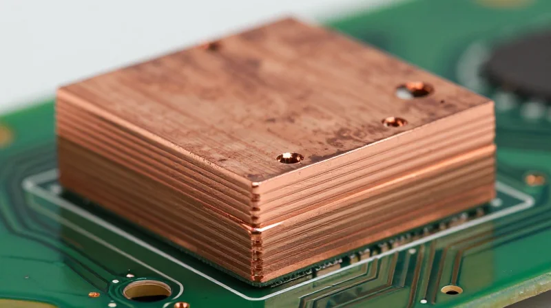
Heavy copper PCBs are defined by copper weights exceeding 3 oz/ft² (105 µm) per layer, often reaching upwards of 30 oz/ft² in specialized power electronics. Unlike standard PCB manufacturing, which focuses on signal integrity and high-density interconnects, heavy copper designs prioritize thermal management and current-carrying capacity. In automotive charging applications, where efficiency and heat dissipation are non-negotiable, heavy copper provides the necessary cross-sectional area to minimize resistive losses ($I²R$) and prevent thermal runaway during continuous high-amperage operation.
Why Standard DFM Rules Fail
Standard DFM guidelines are optimized for thin copper traces where etching factor and plating uniformity are relatively predictable. When transitioning to heavy copper, these conventional assumptions create significant failure points.
| Feature | Standard Copper (0.5-2 oz) | Heavy Copper (3+ oz) |
|---|---|---|
| Etch Factor | High precision, minimal undercut | Significant side-etching risk |
| Thermal Mass | Low, manageable with standard reflow | High, requires specialized pre-heating |
| Solder Mask | Standard clearance suffices | Needs thicker dams for trace isolation |
| Trace Geometry | Vertical, crisp walls | Trapezoidal profiles often inherent |
Frequently Asked Questions
- At what point does a PCB transition from standard to heavy copper?
Industry standards generally classify copper weights of 3 oz/ft² (105 µm) and above as 'heavy.' Designs exceeding this threshold demand unique etching cycles and plating controls. - Why is trace geometry critical in heavy copper?
Due to the long residence time in etching baths required for thick copper, vertical walls are difficult to achieve. Designers must account for trapezoidal cross-sections to ensure calculated current capacity is maintained without risking short-circuits. - Does heavy copper impact layer stack-up selection?
Yes. The increased copper thickness forces higher dielectric spacing to maintain mechanical stability and impedance control, which significantly increases the total board thickness.
Precision Trace Width Calculations for Current Handling
Applying IPC-2221 for High-Current Heavy Copper
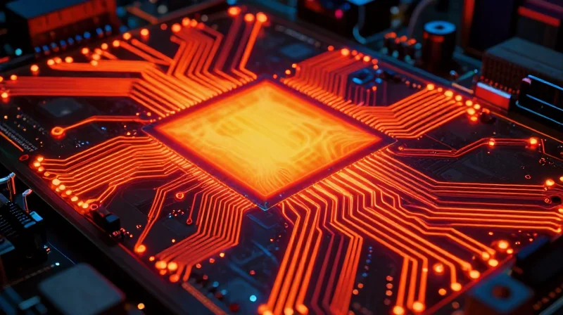
To ensure long-term reliability in automotive charging applications, engineers must move beyond basic design rules and utilize the IPC-2221 standard as the foundational framework for trace geometry. When working with heavy copper—typically defined as 3 oz/ft² or greater—the current-carrying capacity is determined by the intersection of copper thickness, acceptable temperature rise, and the ambient thermal environment. Because high-current traces act as both power conduits and heating elements, DFM strategies must integrate thermomechanical modeling to prevent board delamination or solder joint failure.
Critical Factors in Trace Width Design
| Design Parameter | Impact on Performance | DFM Consideration |
|---|---|---|
| Copper Weight | Determines cross-sectional area | Higher weight allows narrower traces for same current |
| Temperature Rise | Influences material integrity | Standard automotive limit is often 10°C to 20°C |
| Internal vs. External | Heat dissipation efficiency | Internal layers require wider traces due to thermal trapping |
Frequently Asked Questions on Current Handling
- Why does the internal layer width requirement differ from the external layer?
Internal layers are encapsulated by dielectric material, which provides poorer heat dissipation compared to external layers that benefit from convection; therefore, internal traces must be significantly wider to achieve the same temperature rise limit. - Does plating thickness affect the calculation of heavy copper traces?
Yes, standard plating processes add copper to the sidewalls, which changes the effective cross-sectional area. DFM rules must account for these additive tolerances to avoid underestimating current capacity. - How does ambient temperature in an EV charging enclosure impact DFM?
Automotive environments often see elevated ambient temperatures. Designers must derate current capacity based on the difference between the maximum operating ambient temperature and the material's glass transition temperature (Tg).
Advanced Via Strategies for Heat Dissipation
Optimizing Thermal Via Arrays for Heavy Copper
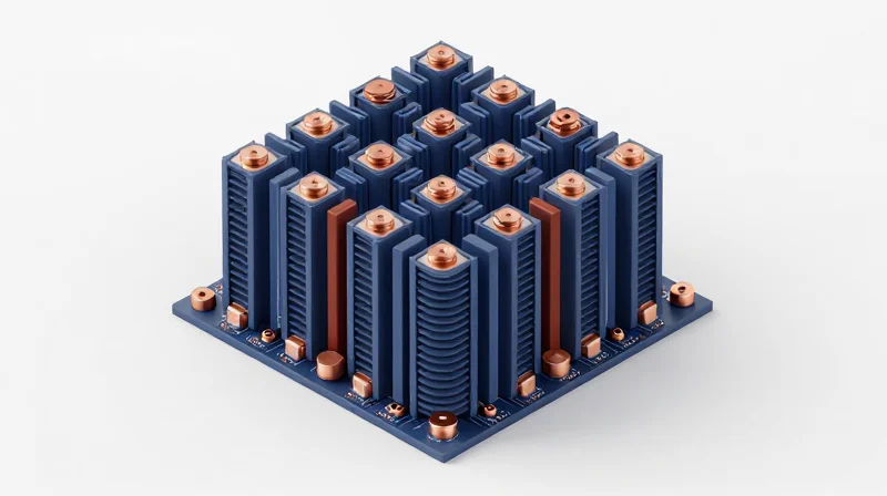
In heavy copper designs, thermal vias act as the primary conduction bridge between internal current-carrying layers and external heat sinks. Effective heat extraction requires a shift from standard signal-via patterns to dense, high-conductivity arrays that prioritize low thermal resistance and structural integrity through the thick copper core.
Strategic Array Configuration
The efficacy of a thermal via array is directly proportional to its total copper volume. For high-current automotive applications, consider these critical design parameters:
- Plating Thickness
Specify a minimum barrel plating thickness of 25 to 35 microns to ensure thermal paths can withstand high-current pulses without necking down or cracking. - Via Filling
Utilize conductive epoxy filling or copper capping (via-in-pad) to maximize the thermal contact surface area at the junction of the component footprint. - Pitch and Density
Maintain a pitch between 0.8mm and 1.27mm to balance heat distribution while preserving the structural rigidity of the PCB substrate.
Thermal Strategy Comparison
| Via Type | Thermal Conductivity | Primary Application |
|---|---|---|
| Standard Thru-Hole | Low | General signal cooling |
| Copper-Capped Via | High | High-power FETs/Rectifiers |
| Conductive Epoxy Filled | Very High | Critical thermal hotspots |
Common Implementation Questions
- How does via diameter affect thermal performance?
Larger diameters increase cross-sectional copper, but can lead to solder wicking issues during assembly; 0.3mm to 0.5mm is generally considered the optimal balance. - Should thermal vias be tied to the ground plane?
Yes, connecting vias to a large internal ground plane distributes heat laterally before it travels to the heatsink, significantly reducing localized stress.
Mitigating PCB Delamination and Stress Fractures
Managing Thermomechanical Stress in Heavy Copper Boards
Heavy copper PCBs generate significant volumetric expansion during thermal cycling, which is the primary driver of delamination and barrel cracking in vias. To mitigate this, engineers must balance the high stiffness of copper with the thermomechanical properties of the substrate. Selecting materials with a high Glass Transition Temperature (Tg) and a low Coefficient of Thermal Expansion (CTE) is essential to maintain structural adhesion between the laminate, resin, and copper layers under extreme automotive operating conditions.
Substrate Material Selection Matrix
| Parameter | Standard FR-4 | High-Tg/High-Performance | Impact on Reliability |
|---|---|---|---|
| Tg | 130°C - 140°C | >170°C | Higher Tg resists resin softening. |
| CTE (Z-axis) | High (>60 ppm/°C) | Low (<40 ppm/°C) | Reduces via barrel stress. |
| T288 | < 5 min | > 10 min | Indicates better thermal shock resistance. |
Preventing Delamination: Best Practices
- Why is CTE matching critical?
The mismatch between copper (17 ppm/°C) and the laminate resin (<60 ppm/°C) causes shear force during thermal expansion. Minimizing this gap reduces the likelihood of pad cratering and delamination. - What role does resin content play?
Use low-resin content (low-flow) prepregs. Excessive resin pockets can create thermal expansion centers that push layers apart during the rapid heating cycles inherent in EV charging. - How does heavy copper geometry influence stress?
Avoid sharp rectangular copper traces where possible. Large copper pours should be cross-hatched or rounded at corners to alleviate localized mechanical stress concentrations in the dielectric material.
Process-Level DFM Recommendations
Beyond material selection, ensure your PCB fabricator employs controlled-depth drilling and increased copper plating thickness in barrels. Because heavy copper boards undergo longer plating cycles, the structural integrity of the copper-to-laminate interface is highly sensitive to the initial etch-back processes. Specifying a 'thick-plating' requirement for internal vias will provide the mechanical ductility necessary to withstand the tensile stress exerted by heavy copper planes during thermal expansion.
Surface Finish Requirements for Power Components
Surface Finish Selection for High-Current Reliability
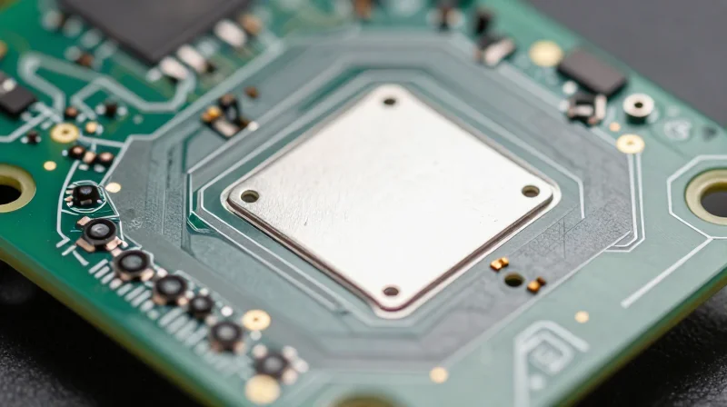
For automotive charging applications, the surface finish must balance solderability, wire-bonding requirements, and long-term resistance to environmental thermal cycling. In heavy copper designs, the primary challenge lies in ensuring that the plating process does not impede the electrical performance or mechanical integrity of high-current junctions.
| Surface Finish | Durability | High-Current Suitability | Recommended Use |
|---|---|---|---|
| ENIG | High | Excellent (Planar) | High-density interconnects and SMT power components |
| HASL (LF) | Medium | Moderate (Uneven) | Large footprint components, legacy designs |
| Immersion Silver | Moderate | Good | High-power busbar connections, press-fit pins |
Comparison of Industry Standards
- Why is ENIG preferred for high-current automotive modules?
ENIG provides a superior, flat surface that ensures consistent solder joint reliability, which is essential for components undergoing high thermal expansion cycles in EV power stages. - Does HASL impact heavy copper board performance?
Yes, traditional HASL can cause uneven surface topology, which leads to poor coplanarity for heavy-duty connectors, potentially creating localized hot spots due to uneven contact resistance. - Is Immersion Silver viable for high-current power stages?
Immersion silver is an excellent choice for press-fit connectors often used in automotive charging, as it provides low contact resistance and excellent conductivity without the risk of nickel-related brittle fractures.
When designing for heavy copper, ensure the plating house accounts for the increased thermal mass of the copper traces during the finish application process. Specifically, ensure that the selected finish does not suffer from 'black pad' syndrome in ENIG applications, which can compromise the integrity of high-power solder joints under vibration stress.
Managing Creepage and Clearance in EV Systems
Defining Creepage and Clearance Constraints
In high-current automotive charging applications, maintaining proper insulation spacing is dictated by standards such as IPC-2221 and IEC 60664-1. Clearance refers to the shortest distance between two conductive parts through air, while creepage is the shortest path along the surface of the solid insulating material. In heavy copper designs, where voltage gradients are significant and contaminants (such as automotive dust or moisture) are prevalent, these physical gaps prevent arcing and tracking.
| Parameter | Primary Risk | Mitigation Strategy |
|---|---|---|
| Clearance | Air Ionization / Arcing | Increase physical gap, conformal coating |
| Creepage | Surface Tracking / Carbonization | Routing slots, surface barriers, CTI-rated materials |
Design Techniques for High-Voltage Isolation
To achieve robust insulation in high-power automotive boards, designers must utilize specific layout techniques beyond basic geometric spacing. The use of milling slots between high-potential traces can effectively increase the creepage distance without expanding the overall PCB footprint. Furthermore, selecting substrates with a high Comparative Tracking Index (CTI) is critical, as materials with higher CTI ratings are less susceptible to forming conductive paths when exposed to electrical stress and environmental pollutants.
Frequently Asked Questions on Isolation
- How does heavy copper affect creepage calculations?
Heavy copper traces have significant thickness, which means the side walls of the copper contribute to the creepage distance. Designers must measure from the edge of the trace cross-section, not just the top surface. - Why is CTI rating important for automotive applications?
Automotive environments often involve high humidity and potential contaminants. A high CTI rating ensures that the PCB laminate remains an insulator even if surface contaminants bridge the gap between traces. - Should I use conformal coating to reduce spacing requirements?
While conformal coating can help, it should generally be viewed as a secondary protective measure rather than a primary solution to reduce clearance requirements, as the coating can degrade or delaminate over time.
DFM Checklist for PCB Fabrication Success
Critical DFM Parameters for Heavy Copper PCBs
Design for Manufacturing (DFM) in heavy copper applications (2 oz to 6 oz+) requires strict adherence to etching, plating, and thermal management constraints. Failing to account for the increased thermal mass and thicker copper geometry often leads to under-etched traces and uneven solder mask coverage.
| Design Constraint | Recommended Practice | Impact on Production |
|---|---|---|
| Copper Spacing | Increase clearance vs. weight | Prevents short circuits during etching |
| Trace Width | Compensate for etch factor | Ensures target impedance/current capacity |
| Via Plugging | Conductive epoxy fill | Prevents solder wicking in high-current vias |
Verification Checklist
- Is the etching compensation factor applied?
Heavy copper widths reduce during etching; verify that your layout tool accounts for the specific copper weight's etch factor to maintain final width tolerances. - Are thermal relief patterns optimized?
Heavy copper acts as a heat sink, making soldering difficult; ensure thermal reliefs are sufficient for assembly without restricting current flow. - Is solder mask registration verified?
Thicker copper requires specialized solder mask application to prevent 'solder mask dams' from failing or creating uneven surface profiles.
Automotive Standard Compliance
Automotive certification often hinges on IPC-2152 compliance. Ensure that all design files include an explicit netlist verification for high-current paths, and confirm with your fabricator that they can maintain internal layer thickness uniformity across large-area copper planes to avoid warpage during the reflow process.
By strictly adhering to these DFM principles, engineers can overcome the challenges inherent in heavy copper PCB design, ensuring maximum safety and efficiency in demanding automotive applications. If you are preparing your design for production and require professional validation, contact our team of experts today for a comprehensive design review.
