
The rapid expansion of the electric vehicle market has placed unprecedented strain on existing charging infrastructure. As we push toward ultra-fast, high-power charging standards, the industry faces a critical bottleneck: how to manage massive current flows without compromising space or thermal efficiency. This article dives into the evolution of power distribution, evaluating why heavy copper technology is becoming the new standard for modern EV charger hardware.
The Evolution of EV Charging Demands
The Transition to High-Voltage Architectures
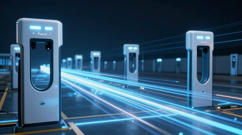
The electric vehicle industry is currently undergoing a pivotal transition from 400V to 800V battery architectures. This shift is primarily driven by the consumer demand for drastically reduced charging times and increased vehicle range. However, higher voltage levels necessitate a fundamental redesign of the power distribution network (PDN), as the existing thermal and space constraints of conventional wiring are quickly becoming the primary bottleneck for vehicle efficiency and charging throughput.
Power Density Constraints
Conventional power distribution, which typically relies on heavy gauge cables, bulky busbars, and discrete connectors, struggles to keep pace with the power density requirements of next-generation chargers. As charging power requirements soar beyond 350kW, traditional wiring methods face significant challenges regarding mass, volumetric footprint, and heat dissipation. The following table highlights the critical limitations of current methods versus the adoption of heavy copper PCBs.
| Feature | Conventional Busbars | Heavy Copper PCBs |
|---|---|---|
| Integration | Discrete/External | Embedded/Modular |
| Thermal Dissipation | High (Requires Cooling) | Superior (Integrated Plane) |
| Space Efficiency | Low | High |
| Automation Potential | Manual Assembly | Full SMT Compatibility |
Addressing Emerging Technical Challenges
- Why is 800V causing thermal challenges in traditional systems?
While higher voltage reduces current for the same power, the rapid switching frequencies of SiC-based power electronics generate localized high-heat zones that traditional, multi-piece busbar assemblies cannot effectively dissipate. - How do heavy copper PCBs solve space constraints?
Heavy copper PCBs integrate high-current traces directly into the substrate, eliminating the need for bulky wiring harnesses and complex connectors, thereby saving critical vehicle chassis volume. - Is reliability improved with PCB-based power distribution?
Yes, by replacing mechanical crimps and fasteners with integrated board-level connections, manufacturers significantly reduce the number of potential failure points caused by vibration and thermal expansion.
Understanding Traditional Power Distribution Designs
The Bottlenecks of Conventional PCB Power Distribution
Standard power distribution in EV infrastructure has historically relied on multilayer printed circuit boards (PCBs) utilizing standard copper weights (typically 1oz to 3oz). While sufficient for lower-power logic and control systems, these designs create a thermal and resistive bottleneck when tasked with the continuous high-amperage loads required by 800V DC fast-charging stations. The primary limitation stems from the cross-sectional area of the copper traces, which induces significant I²R (resistive) heating, potentially leading to localized hotspots, material degradation, and ultimately, system failure.
Thermal Dissipation and Resistance Constraints
In conventional designs, the thickness of copper is often sacrificed to allow for finer feature sizes required for complex circuitry. However, current-carrying capacity is directly proportional to the cross-sectional area. As amperage increases, these thinner traces encounter significant resistance, requiring designers to compensate with larger board footprints or costly active cooling solutions. This creates a cycle of inefficiency where the infrastructure requires larger, heavier heat sinks, undermining the goal of compact, high-density power electronics.
| Parameter | Standard PCB (1-2oz) | Impact on EV Infrastructure |
|---|---|---|
| Current Density | Low/Moderate | Requires oversized copper planes |
| Thermal Management | Active Cooling Required | Increases total system weight/volume |
| Reliability | Susceptible to hotspots | Higher risk of substrate delamination |
Common Industry Challenges
- Why do standard PCBs fail under high-amperage loads?
The limited thickness of standard copper leads to increased resistive heating, which can exceed the thermal limits of the FR-4 substrate material. - How does trace width affect layout efficiency?
To carry higher current, designers must widen traces significantly, which complicates component routing and limits the density of the overall power module. - Is active cooling the best solution for standard PCBs?
Active cooling adds weight, cost, and a point of mechanical failure, making it an suboptimal solution for the longevity and reliability requirements of public EV charging stations.
The Role of Busbars in Modern Charging Stations
The Engineering Necessity of Busbars
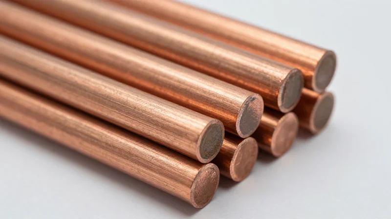
As electric vehicle charging stations push toward higher power thresholds, traditional cabling and standard PCB traces often reach physical thermal limits. Busbars—solid, flat conductors made of copper or aluminum—provide an efficient, low-resistance path for high-amperage current. In the context of 800V architectures, these components minimize inductive losses and provide structural rigidity, which is essential for managing the heat generated by rapid charge cycles.
Busbars vs. Conventional PCB Distribution
| Feature | Busbar Technology | Conventional PCB |
|---|---|---|
| Current Capacity | Very High (hundreds of Amps) | Limited by trace width |
| Thermal Dissipation | Excellent (Surface area) | Requires extensive cooling |
| Form Factor | Bulky and Rigid | Compact and Flexible |
| Assembly Effort | High (Fasteners/Bending) | Low (Automated SMT) |
Trade-offs in Integration
While busbars outperform PCBs in power density, they introduce significant design challenges regarding space constraints and assembly automation. Unlike a heavy copper PCB, which can be processed in a standard pick-and-place manufacturing line, busbars often require custom stamping, bending, and mechanical fastening. This necessitates a hybrid approach where high-power stages are handled by busbars while control signals remain on PCBs.
Frequently Asked Questions
- Why not use copper PCBs for everything?
Even with heavy copper (e.g., 6oz or higher), PCBs suffer from dielectric degradation under high thermal stress and have lower cross-sectional areas compared to solid busbars, leading to increased resistance at extreme currents. - How do busbars improve system reliability?
Busbars offer a lower risk of fatigue and connection failure compared to soldered PCB joints, especially in environments exposed to the vibration and thermal cycling common in industrial charging hardware. - Is there a future for integrated busbar-PCBs?
Yes, industry trends are moving toward embedded busbar technologies, where conductors are laminated directly into the PCB stack-up to combine the high-current advantages of busbars with the assembly ease of electronics boards.
Introduction to Heavy Copper PCB Technology
Defining Heavy Copper PCB Architecture
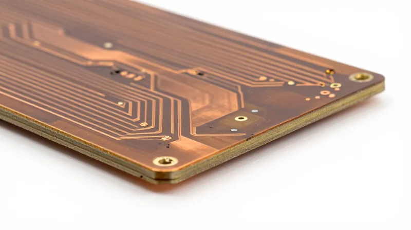
Heavy copper PCBs are defined by copper weights exceeding 3 ounces (oz) per square foot, with industrial applications often scaling up to 20 oz or more. Unlike standard rigid boards—which typically utilize 0.5 oz to 2 oz of copper—these specialized PCBs serve as integrated power distribution components. By utilizing thicker copper traces, manufacturers can significantly reduce electrical resistance, minimize voltage drops, and improve heat dissipation across the conductive path.
Manufacturing Advancements for High-Power Reliability
The evolution of high-amperage PCB design is driven by advanced etching techniques and specialized electroplating processes. Manufacturing thick copper requires precise control over the undercut during the etching process to maintain trace geometry. Furthermore, advanced thermal management materials, such as high-Tg (glass transition temperature) laminates, are employed to withstand the localized thermal stresses inherent in high-current EV charging infrastructure.
| Feature | Standard PCB | Heavy Copper PCB |
|---|---|---|
| Copper Weight | 0.5 - 2 oz | 3 - 20+ oz |
| Current Capacity | Low/Moderate | Very High |
| Thermal Dissipation | Limited | Excellent |
| Primary Application | Signal/Data Processing | Power Electronics/EV Charging |
Frequently Asked Questions
- At what point is a PCB classified as 'Heavy Copper'?
A PCB is generally classified as heavy copper when the copper layer weight exceeds 3 ounces per square foot, though specialized applications may start at 4 oz. - How does heavy copper affect board thickness?
Due to the increased thickness of the copper traces, these PCBs require deeper etched channels and thicker base laminates to ensure mechanical integrity and insulation performance under high-voltage loads. - Can heavy copper replace all busbars in EV chargers?
In many mid-to-high power density applications, yes. Integrating power paths into the PCB reduces manual assembly time, lowers connection points, and decreases overall system volume compared to discrete busbar installations.
Efficiency Metrics: Heavy Copper vs. Traditional Busbars
Comparative Efficiency Metrics
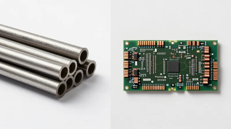
Transitioning from discrete busbar assemblies to heavy copper PCB architectures represents a fundamental shift in power distribution. By integrating high-current paths directly onto the substrate, manufacturers can reduce the volumetric footprint of the power stage, minimize parasitic inductance, and optimize thermal management in high-amperage EV charging environments.
| Metric | Traditional Busbar Systems | Heavy Copper PCBs (>3oz) |
|---|---|---|
| Form Factor | High volume, rigid geometry | Low profile, compact footprint |
| Assembly Complexity | High (mechanical fasteners/welding) | Low (automated SMT assembly) |
| Thermal Conductivity | High localized heat sinking | Distributed heat dissipation |
| Weight Impact | Significant, structural overhead | Minimal, integrated design |
Key Performance Advantages
- Does weight reduction matter for stationary charging?
While stationary, reducing total system mass lowers shipping costs and allows for less robust, more cost-effective enclosure designs, which directly impacts the total cost of ownership. - How does integration improve thermal performance?
Heavy copper PCBs allow for a larger conductive surface area closer to the heat source, reducing thermal resistance by eliminating the interface layers required between discrete busbars and components. - What is the impact on parasitic inductance?
By shortening conductive paths and enabling closer proximity between power components, heavy copper PCBs significantly reduce loop inductance, leading to cleaner switching and higher efficiency in power converters.
Ultimately, the selection between these technologies hinges on the power density requirements of the specific EV charging application. While busbars remain the standard for extreme, continuous high-current industrial power delivery, heavy copper PCBs provide a superior balance of intelligence and power, enabling the next generation of modular, compact, and high-efficiency charging infrastructure.
Overcoming Thermal Management Bottlenecks
In conventional high-power EV systems, thermal bottlenecks often stem from the reliance on discrete busbars and external heat sinks, which create localized hot spots and increase thermal resistance at connection interfaces. By leveraging heavy copper PCBs, manufacturers can transition from discrete components to integrated power distribution that utilizes the copper planes themselves as primary heat-spreading conduits.
Heat Dissipation Through Integrated Copper Planes
The primary advantage of heavy copper (>3oz) lies in the increased thermal conductivity provided by the expanded cross-sectional area. Unlike thin-trace PCBs that act as thermal resistors, heavy copper internal layers serve as heat spreaders that draw energy away from high-power MOSFETs and IGBTs directly into the board substrate. This lateral heat distribution lowers the junction temperature of power semiconductors, directly extending component lifespan and allowing for higher current density without increasing the total system volume.
| Feature | Conventional Busbar Systems | Heavy Copper PCB Integration |
|---|---|---|
| Thermal Resistance | High (Interfacial losses) | Low (Monolithic conduction) |
| Heat Distribution | Localized/Point-based | Uniform/Area-based |
| External Cooling | Significant requirements | Reduced or eliminated |
Strategic Advantages in Thermal Design
- How do internal heavy copper layers mitigate hot spots?
The increased copper mass facilitates rapid lateral heat spreading across the entire PCB surface, preventing the thermal stacking common in high-density components. - Does heavy copper eliminate the need for thermal interface materials (TIM)?
While it does not eliminate the need for TIM entirely, it significantly reduces the reliance on thick, high-resistance TIM layers by allowing the PCB to mount directly to a chassis or integrated cold plate with greater surface uniformity. - What impact does this have on EV system weight?
By replacing heavy copper busbars and bulky mechanical mounting hardware with a high-current PCB, OEMs can achieve a net reduction in system weight while maintaining superior thermal stability.
Reliability and Longevity in Field Deployments
Durability Under Extreme Environmental Cycling
EV charging stations are subjected to rigorous thermal cycling, with internal components repeatedly oscillating between ambient temperatures and peak operating heat during high-load charging sessions. Conventional power distribution, often reliant on mechanical interconnects, busbars, and fasteners, is susceptible to thermal expansion and contraction. This movement can lead to creep or loosened contacts over time. In contrast, heavy copper PCBs utilize integrated conductive paths and solder-alloy connections that provide a monolithic structural integrity, drastically reducing the points of failure and maintaining low-resistance paths even after thousands of charge cycles.
Reliability Comparison: Heavy Copper PCBs vs. Discrete Busbars
| Failure Factor | Discrete Busbar Assemblies | Heavy Copper PCBs |
|---|---|---|
| Mechanical Vibration | Potential for loosened connections | High structural stability |
| Thermal Expansion | High risk of interface fatigue | Minimal coefficient mismatch |
| Maintenance Needs | Periodic retightening required | Maintenance-free design |
| Oxidation Exposure | Visible contact points prone to corrosion | Enclosed, protected conductive layers |
Operational Longevity and Maintenance
By shifting power distribution onto the PCB itself, manufacturers eliminate the need for cumbersome wiring harnesses and point-to-point busbar connections. This not only improves long-term reliability by minimizing the human-error factor during assembly but also enhances the overall electromagnetic compatibility (EMC) of the charging station. The reduction in localized hot spots—achieved through the planar nature of heavy copper—prevents accelerated aging of adjacent electronic components, such as MOSFETs and capacitors, thereby extending the MTBF (Mean Time Between Failures) of the entire charging unit.
Frequently Asked Questions
- How does heavy copper reduce long-term maintenance costs?
By removing mechanical fasteners and discrete busbar interconnections, heavy copper PCBs eliminate the risk of connection fatigue, effectively removing the need for scheduled maintenance checks of electrical contact points. - Is heavy copper susceptible to solder fatigue during thermal cycling?
When designed with appropriate trace geometry and balanced copper distribution, the PCB acts as a thermally stable platform that mitigates mechanical stress on solder joints, ensuring better long-term reliability than traditional bolted systems. - What is the expected service life of a high-copper power board?
Under standard industrial operating parameters, heavy copper PCBs are engineered to last the full lifecycle of the EV charging station, often exceeding 10 to 15 years, provided the thermal design remains within recommended limits.
Cost-Effectiveness and Manufacturing Scalability
Economic Analysis: Initial Capital vs. Operational Efficiency
While heavy copper PCBs require higher precision in raw material procurement and specialized fabrication processes compared to traditional busbars, the long-term cost-effectiveness is driven by reduced assembly complexity. By consolidating power distribution, control logic, and sensing into a single monolithic substrate, manufacturers eliminate the manual labor associated with bending, bolting, and insulating discrete copper rods.
| Feature | Conventional Busbars | Heavy Copper PCB |
|---|---|---|
| Material Cost | Low | Moderate |
| Assembly Labor | High | Low |
| Tooling Flexibility | Low | High |
| Total Cost of Ownership | Moderate | Lower (at scale) |
Manufacturing Scalability and Automation
Scalability in EV infrastructure deployment relies on standardized, automated assembly. Conventional power distribution often requires custom mechanical fittings that are difficult to automate on high-speed lines. Heavy copper PCB technology leverages established surface-mount and through-hole automation, allowing for a seamless transition from prototype to mass production without the need for extensive mechanical retooling.
Frequently Asked Questions on Economic Scalability
- Does the complexity of multi-layer heavy copper increase waste?
Modern fabrication processes, such as advanced etching and laser direct imaging, have significantly reduced material waste, making high-layer-count heavy copper boards increasingly cost-competitive for high-current applications. - Why is the transition toward PCBs preferred for mass-market chargers?
PCBs offer repeatable quality and integrated diagnostic capabilities, which significantly lowers field maintenance and diagnostic costs over the multi-year lifecycle of public charging stations. - Can current PCB fabrication infrastructure support high-copper volume?
Yes, many tier-one board manufacturers have expanded their capacity for 3oz to 6oz+ copper plating, aligning production capabilities with the demand for robust EV power distribution.
Future-Proofing Your EV Infrastructure Strategy

Adopting a Hybrid Strategy for Scalable Power
To achieve long-term viability in EV infrastructure, design engineers must transition away from rigid, legacy distribution methods toward hybrid PCB architectures. By integrating heavy copper layers directly into the power delivery network, engineers can maintain extreme power density while utilizing modular components for easier field maintenance and future upgrades.
Comparative Analysis: Hybrid Design vs. Conventional Busbars
| Feature | Conventional Busbar | Hybrid Heavy Copper PCB |
|---|---|---|
| Integration | External/Discrete | Embedded/Integrated |
| Space Efficiency | Low | High |
| Thermal Management | Conduction-only | PCB-Plane Dissipation |
| Field Repairability | Moderate | High (Module Swapping) |
Key Considerations for Design Engineers
- How do I balance copper thickness with fabrication constraints?
Utilize 3oz to 6oz copper weights for primary distribution and transition to standard weights for signal layers to keep fabrication costs optimized without sacrificing conductivity. - What is the best approach to ensure mechanical stability?
Incorporate reinforced glass-epoxy substrates with high Tg (glass transition temperature) ratings to prevent thermal warping during high-amperage charging cycles. - Is modularity achievable with PCB-based power?
Yes, by utilizing press-fit connector technology on heavy copper boards, you eliminate the need for wave soldering while enabling rapid field-replaceable unit (FRU) maintenance.
The transition to heavy copper PCB architectures is not merely a cost-saving measure; it is a design imperative for modern EV charging stations. By standardizing on modular, high-copper-density platforms, manufacturers can ensure their infrastructure remains adaptable to evolving grid requirements and higher vehicle-to-grid (V2G) power demands.
Selecting the right power distribution technology is no longer just about current capacity; it is about balancing heat management, form factor, and long-term reliability. As the industry advances, heavy copper PCBs provide a compelling pathway for smaller, more efficient charger architectures. Contact our engineering team today to evaluate how high-performance PCB solutions can elevate your next generation of EV infrastructure projects.
