In today's fast-paced electronics industry, reliable and cost-effective PCB manufacturing is crucial. JLCPCB, a prominent player in this field, offers a range of services from rapid prototyping to full-scale PCB assembly. This article dives into the world of JLCPCB, exploring its offerings and how it facilitates innovation and production across the globe, helping to connect technology with daily life. We’ll cover key aspects, from its manufacturing capabilities to its advantages in the market, guiding both new and experienced users.
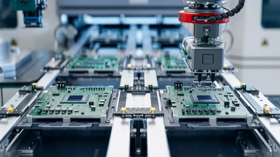
JLCPCB has established itself as a prominent global leader in printed circuit board (PCB) manufacturing, tracing its origins back to 2006 in Shenzhen, China. The company's trajectory from a local entity to a major international player in the electronics industry is a testament to its commitment to innovation, quality, and customer-centric practices.
Founded with a vision to streamline the PCB manufacturing process, JLCPCB has leveraged technological advancements and a robust supply chain to offer a comprehensive suite of services, ranging from rapid PCB prototyping to large-scale production. This approach has enabled the company to cater to diverse customer needs, from individual hobbyists to large-scale industrial clients.
Key milestones in JLCPCB's growth include the expansion of its manufacturing capabilities, the development of an efficient online ordering system, and the implementation of stringent quality control measures. These efforts have not only enhanced its operational efficiency but have also strengthened its reputation as a trusted and reliable PCB manufacturing partner worldwide.
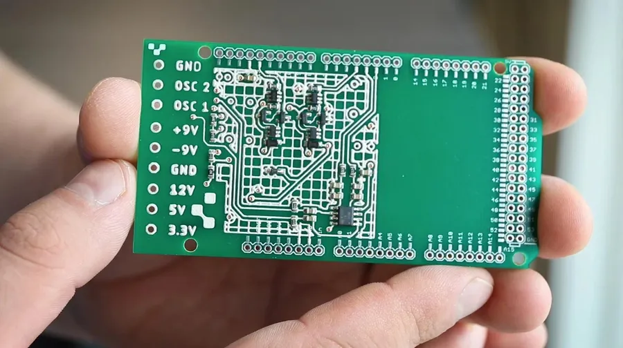
JLCPCB provides a comprehensive suite of services encompassing the entire PCB lifecycle, from initial prototyping to full-scale production and assembly. These services are designed to cater to a wide spectrum of needs, ranging from simple, single-sided boards to complex, multi-layered designs with advanced assembly requirements. Their offerings cover PCB prototyping, fabrication, SMT assembly, and stencil production, allowing for a streamlined process from design to finished product.
| Service | Description | Typical Applications |
|---|---|---|
| PCB Prototyping | Rapid manufacturing of small quantities of PCBs for testing and validation. This service is essential for quickly iterating designs. | Early-stage product development, circuit verification, proof-of-concept models. |
| PCB Fabrication | Manufacturing PCBs in larger volumes according to customer specifications. Can handle a variety of board types, from single-layer to multi-layer designs, and various materials. | Mass production of electronics, manufacturing of commercial products, complex devices requiring specialized PCBs. |
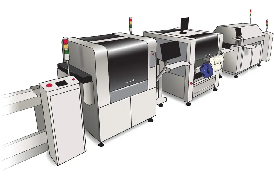
| SMT Assembly | Automated surface mount technology assembly of components onto PCBs. Can handle a wide variety of components. It includes both manual pick-and-place and reflow soldering for automated volume assembly. | Final product assembly, complex electronic devices, and situations where manual assembly isn't practical. |
| Stencil Production | Manufacturing of stencils used in applying solder paste on PCBs during SMT assembly. These stencils ensure precise application of paste for quality assembly. | Preparation for SMT assembly, projects that need controlled solder paste deposition, mass production of SMT assemblies. |
Selecting the right PCB manufacturer is crucial for the success of any electronics project. JLCPCB distinguishes itself by offering a compelling combination of cost-effectiveness, rapid turnaround times, and high-quality manufacturing. This section delves into these advantages, providing a clear picture of why JLCPCB is a preferred choice for many.
JLCPCB's commitment to providing cost-effective PCB manufacturing is evident through their competitive pricing structures. They achieve this through economies of scale and efficient production processes, ultimately benefiting their customers with lower costs for both prototype and mass production runs. This allows projects, especially smaller ones, to become more feasible financially. Furthermore, the speed at which they process and deliver PCBs is a significant advantage. JLCPCB's optimized workflow, including quick online quoting, production and shipping, ensures that customers receive their boards in a short amount of time. This is particularly beneficial in fast-paced environments where time to market is critical.
Despite their competitive pricing and rapid production, JLCPCB does not compromise on the quality of their manufactured PCBs. Their focus on maintaining high standards is achieved through rigorous quality control measures and the use of advanced manufacturing equipment, assuring that each board complies with the required specifications and performance demands. The combination of these factors positions JLCPCB as a strong contender, especially when compared to major market competitors. These three factors provide a compelling argument for making them the manufacturer of choice. The subsequent section provides a comparison with some of the most common competitors to further support this claim.
| Advantage | Description | Impact |
|---|---|---|
| Cost-Effectiveness | Competitive pricing and volume discounts | Reduced project costs, making projects more financially viable |
| Rapid Turnaround | Fast online quoting, efficient production and expedited shipping. | Faster project completion and quicker time to market. |
| High-Quality Manufacturing | Rigorous quality control measures and advanced equipment | High reliability and fewer defects in PCB production |
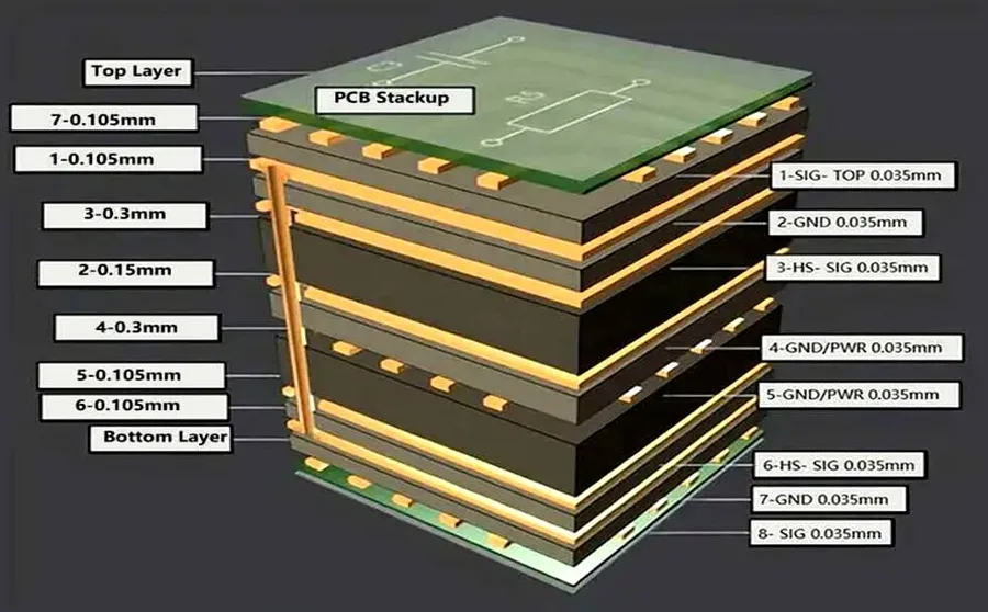
JLCPCB's manufacturing prowess is defined by its ability to handle a wide spectrum of PCB designs, ranging from simple single-layer boards to intricate multi-layer constructions. Their capabilities span various materials, layer counts, and precision tolerances, making them a versatile partner for diverse electronic projects. JLCPCB demonstrates robust capacity for both prototyping and mass production.
| Capability | Details | Significance |
|---|---|---|
| Material Options | FR-4, Aluminum, Rogers, etc. | Enables selection of appropriate material based on application requirements (e.g., thermal, electrical, mechanical). |
| Layer Count | 1 to 16 layers standard, up to 20 layers on request | Accommodates diverse design complexities, from basic circuits to sophisticated multilayer designs. |
| Copper Thickness | 1oz, 2oz, up to 3oz on request | Meets current-carrying requirements for varied applications. |
| Minimum Track Width/Spacing | 0.076mm / 0.076mm (3mil) | Enables high-density circuit layouts and miniaturization of devices. |
| Minimum Hole Size | 0.2mm | Accommodates fine-pitch components and intricate board features. |
| Board Thickness | 0.4mm to 3.2mm | Offers a range of options for different mechanical requirements and housing needs. |
| Surface Finishes | HASL, ENIG, Immersion Tin, Immersion Silver, OSP | Provides options for solderability, corrosion resistance, and long-term reliability. |
| Solder Mask Colors | Green, Red, Yellow, Blue, White, Black, Matte Black | Allows for visual identification and organization within electronic systems. |
| Precision Tolerances | IPC Class 2 standards compliance, with options for tighter tolerances | Ensures quality, reliability and consistent performance of PCBs. |
| Specialized Processes | Blind and buried vias, controlled impedance | Supports complex design needs and specialized applications. |
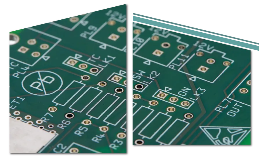
JLCPCB has streamlined its ordering process to ensure a user-friendly experience, from initial design upload to final order placement. Their online platform is designed to be intuitive, allowing both seasoned professionals and hobbyists to easily navigate the process of obtaining custom PCBs. The focus is on clarity and efficiency, guiding users through each step of the PCB manufacturing journey.
This section addresses common questions regarding JLCPCB, offering clarity on its operational aspects, geographical location, ownership, and its standing in the global PCB manufacturing sector. It aims to provide comprehensive answers to frequently asked questions, offering a clear understanding of JLCPCB's operations and position in the industry.
JLCPCB is actively shaping the future of PCB manufacturing through strategic investments in cutting-edge technologies and sustainable practices. Their forward-thinking approach aims to solidify their position as a market leader by adapting to emerging trends and continually enhancing their capabilities.
Their commitment extends beyond traditional PCB fabrication, encompassing advancements in digital integration and eco-conscious manufacturing. This positions them not just as a manufacturer, but as a significant contributor to the evolution of the electronics industry.
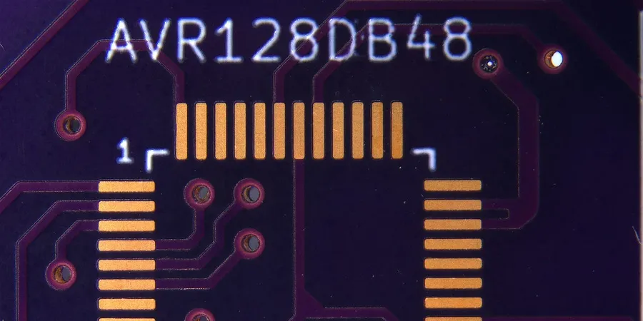
Choosing the right PCB manufacturer is crucial for any electronics project, and a comparison of key players like JLCPCB and PCBWay is essential for informed decision-making. This section provides a balanced analysis of these two manufacturers across critical factors, enabling engineers and designers to select the optimal partner for their specific needs.
| Feature | JLCPCB | PCBWay |
|---|---|---|
| Price | Generally very competitive, especially for prototypes and small batches. | Competitive pricing, with options for various scales of production. |
| Turnaround Time | Fast turnaround times, especially for standard specifications. | Good turnaround times, similar to JLCPCB, with express options available. |
| Quality | Good quality PCBs, with rigorous testing processes, offering good value for money. May experience slight variances in very high-density or complex designs. | High-quality PCBs with very good tolerances. Consistent quality, particularly for more demanding applications and complex designs, often at a premium price. |
| Service Offerings | Comprehensive services including PCB prototyping, fabrication, assembly, and stencil services. Strong focus on online ordering and automated processes. | Wide range of services including PCB prototyping, fabrication, assembly, CNC machining and 3D printing. Offers more customization and tailored solutions. |
| Customer Support | Generally responsive, with online support via their platform. | Strong customer support with options for direct communication and technical assistance. |
| Capabilities | Suitable for a wide range of projects, with capabilities for multi-layer PCBs, SMT assembly, and various materials. | Good capabilities for complex designs, high layer counts, and advanced materials, with additional services like CNC and 3D printing. |
In summary, JLCPCB is an excellent choice for cost-conscious projects, offering quick turnaround for standard PCBs. PCBWay shines in situations demanding higher levels of customization, technical support, and consistency in quality for complex designs, albeit at a generally higher price point. The ideal manufacturer ultimately depends on the specific priorities of the project.
JLCPCB stands out as a reliable and cost-effective PCB manufacturer, providing rapid prototyping and assembly services to meet diverse needs across the electronics industry. With its commitment to innovation and digital systems, JLCPCB is well-positioned to continue leading the way in PCB manufacturing. Whether you are a hobbyist or a large-scale manufacturer, JLCPCB offers a compelling solution for your PCB requirements, contributing significantly to the technological advancements that shape our world. JLCPCB empowers electronics innovation with its fast, reliable, and affordable PCB manufacturing services.

