In today's fast-paced world of electronics, reliable and cost-effective PCB manufacturing is crucial. JLCPCB has emerged as a significant player, offering prototyping and assembly services to engineers and hobbyists worldwide. From complex circuit boards powering cutting-edge devices to simple boards for DIY projects, JLCPCB's impact is undeniable. This article serves as your comprehensive guide to understanding JLCPCB, its services, and how to leverage them for your next project.
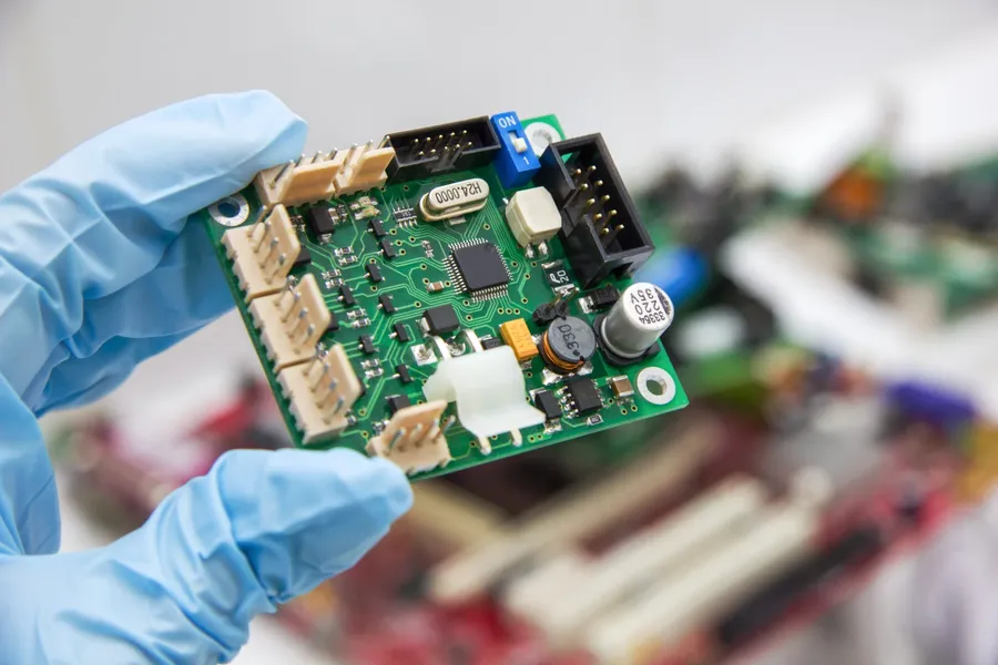
JLCPCB has rapidly become a prominent player in the global PCB (Printed Circuit Board) manufacturing industry, providing cost-effective and efficient solutions for prototyping and production. Established in 2006, the company has focused on leveraging technology to streamline PCB fabrication and assembly, appealing to a diverse clientele from hobbyists to large-scale enterprises. Their commitment to high quality and rapid turnaround times has cemented their position as a leading PCB provider.
JLCPCB's core mission revolves around offering accessibility to advanced PCB technologies. They aim to reduce the barriers to entry for individuals and organizations seeking custom circuit boards, while also maintaining stringent quality standards. The company's global reach extends across numerous countries, serving a wide array of customers ranging from individual electronics enthusiasts and academic institutions to industrial companies requiring printed circuit boards for their commercial products. This wide customer base reflects JLCPCB's versatile approach to PCB production.
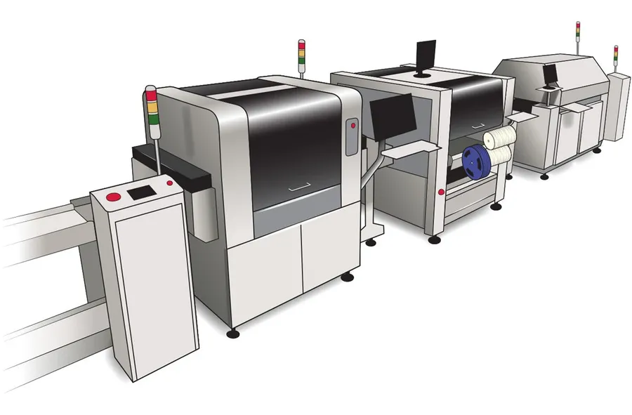
JLCPCB excels in providing rapid and reliable PCB prototyping and fabrication services, catering to a wide spectrum of needs from simple single-layer boards to complex multi-layer designs. Their core strength lies in balancing affordability with high-quality manufacturing, making them a popular choice for both hobbyists and professional engineers.
| Feature | Details | Typical Specification | Options Available |
|---|---|---|---|
| Layer Count | Number of conductive layers in the PCB. | 1 to 4 layers standard | 1-20 layers or more available |
| Material Choices | Base material used to construct PCB | FR-4 standard | Aluminum, Rogers, Flexible PCB options also available |
| PCB Thickness | Thickness of the base material used | 1.6mm standard | 0.4mm - 2.0mm and other thickness available |
| Minimum Track Width/Spacing | Smallest allowable trace width and spacing between traces | 6mil (0.1524mm) standard | 4mil (0.1016mm) possible in advanced manufacturing options |
| Surface Finish | Protective coating applied to exposed copper | HASL standard | ENIG, Immersion Tin, OSP available |
| Copper Weight | Thickness of the copper layers on the PCB | 1oz standard | 2oz copper available |
| Manufacturing Standards | Adherence to industry guidelines and best practices | IPC-A-600 Class 2 standard | Class 3 possible for special orders |
| Turnaround Time | Time taken to complete fabrication process | 24 Hours for some services | Expedited and standard manufacturing times |
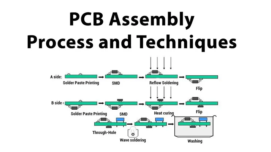
JLCPCB provides comprehensive PCB assembly services, encompassing both Surface Mount Technology (SMT) and Through-Hole assembly, catering to a wide range of electronic manufacturing needs. This service enables customers to move beyond bare board fabrication to fully assembled and functional circuit boards, streamlining the production process. By offering both SMT and through-hole capabilities, JLCPCB supports diverse project requirements, accommodating both modern, miniaturized components as well as more traditional through-hole parts.
JLCPCB's assembly service includes component sourcing, automated pick-and-place for SMT, and manual or automated assembly for through-hole components. JLCPCB maintains a stock of commonly used 'basic parts', which can simplify component selection and sourcing for many customers. For specific projects that need additional or custom components, the customer is able to source these parts and send them to JLCPCB. Proper file preparation is critical for a successful PCB assembly process, requiring both a Bill of Materials (BOM) and a Component Placement List (CPL).
| Feature | SMT Assembly | Through-Hole Assembly |
|---|---|---|
| Component Type | Surface mount components | Leaded components |
| Assembly Process | Automated pick-and-place | Manual or automated insertion |
| Component Sourcing | JLCPCB basic parts or customer supplied | JLCPCB basic parts or customer supplied |
| File Requirements | BOM and CPL files | BOM file |
To accurately prepare your files for assembly with JLCPCB, you should ensure your BOM lists every component, including the part number, manufacturer, and quantities. The CPL file is necessary for SMT assembly, providing the X and Y coordinates, rotation, and designator for each component so the automated assembly machines know how and where to place them on the PCB.
Understanding JLCPCB's pricing structure is crucial for cost-effective PCB fabrication and assembly. JLCPCB offers competitive pricing, but costs vary based on several factors including order volume, PCB complexity (number of layers), and required assembly services. This section provides a detailed analysis of these cost factors to help you optimize your designs and minimize expenses.
| Factor | Description | Impact on Cost |
|---|---|---|
| Order Volume | Number of PCBs ordered in a single batch. | Higher volumes generally result in lower per-unit cost. |
| Number of Layers | The number of conductive layers in the PCB (e.g., 1, 2, 4, 6 layers). | Increased layers directly increase fabrication complexity and cost. |
| Board Dimensions | The size of the PCB. | Larger boards generally increase cost due to increased material and fabrication time. |
| PCB Material | Standard FR-4 is most common but other materials like aluminum or flex may be selected | Advanced materials command higher prices than standard FR-4 materials |
| PCB Thickness | Standard PCB thickness is 1.6mm with other options available | Non-standard thickness may affect pricing. |
| Assembly Complexity | Complexity of the assembly (e.g., number of components, SMT vs. through-hole). | More complex assemblies lead to higher costs for component placement. |
| Component Sourcing | Whether components are supplied by the user or sourced by JLCPCB (basic components vs extended parts) | Using Basic components from JLC inventory reduce component cost, Using Extended parts and user supply increase cost |
| Turnaround Time | The production speed required (standard vs expedited). | Faster turnaround times may incur additional charges. |
JLCPCB typically offers tiered pricing, with significant discounts for larger order quantities. For example, a small batch of 5 PCBs might cost more per unit than an order of 100 PCBs. Similarly, a four-layer board will cost significantly more than a two-layer board due to the added complexity in manufacturing. Understanding these tiered pricing schemes is essential for budget optimization.
For PCB assembly, the cost is influenced by the number of components, the type of components (SMT or through-hole), and whether JLCPCB sources the components or you supply them. JLCPCB offers 'basic' components in their inventory for a low cost, but for specialized parts you may need to source and supply. Using components from JLCPCB's basic parts library significantly reduces the cost of the assembly.
Here are some tips for optimizing your design to minimize cost:
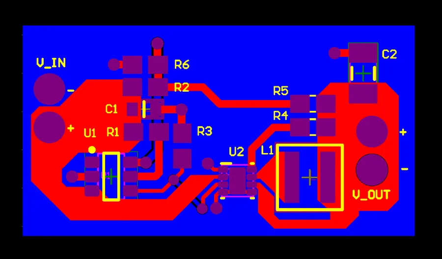
Ordering PCBs from JLCPCB involves a structured process, from preparing your design files to finalizing your order. This guide will provide a practical, step-by-step approach to ensure a smooth and successful experience. The process includes preparing your design files, configuring your order on the JLCPCB website, and reviewing your Gerber files.
Key aspects to check when reviewing your Gerber files include ensuring that all the design layers are present, drill holes are correctly positioned, and the overall dimensions and board shape are accurate. Pay close attention to the clearance between traces and pads. It is crucial that all the design rules of your design are adhered to, as any violations will lead to failure of the PCB.
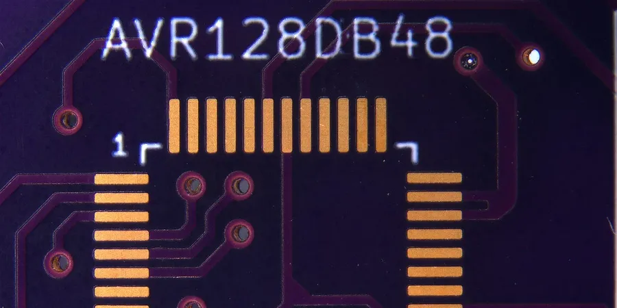
Choosing the right PCB manufacturer is critical for any electronics project, and JLCPCB often stands out as a strong contender. However, a comprehensive assessment necessitates comparing it against its competitors, such as PCBWay. This section provides a structured comparison of JLCPCB with other manufacturers, focusing on key factors like pricing, lead times, capabilities, and customer support, to help you make an informed decision.
| Feature | JLCPCB | PCBWay |
|---|---|---|
| Pricing | Generally lower for prototyping and small batches; tiered pricing available. | Competitive but may be higher for small quantities; varied pricing options. |
| Lead Times | Typically offers quick turnaround times, especially for standard PCBs. | Similar lead times, with expedited options available. |
| PCB Capabilities | Offers a wide range of options, including multi-layer boards, various materials, and advanced features, but can be limiting on complex designs. | Provides a broader range of material options, including advanced materials. More tolerance on complex designs. |
| Assembly Capabilities | Strong in SMT assembly, with a good selection of basic parts readily available; can source custom components. | Comprehensive assembly options including through-hole and advanced component sourcing. |
| Customer Support | Generally responsive and helpful; online support and ticketing system. | Strong customer support with dedicated account managers and faster response times. |
| Component Sourcing | Good selection of basic parts, but specialized components may require external sourcing. | More extensive component sourcing capabilities, including hard-to-find components. |
| Minimum Order Quantity | Low minimum order quantity, beneficial for small projects and prototyping. | Varies with service, can be higher than JLCPCB. |
| Shipping | Good shipping options, with tracking and express options available. | Reliable shipping options, with varied international delivery times. |
| Ease of Use | Straightforward ordering process, user-friendly interface. | Slightly more complex ordering process for beginners. |
This section addresses common queries about JLCPCB, providing clear and concise answers to help users understand the company, its operations, and the services it provides. We've incorporated common 'People Also Ask' questions to offer a comprehensive overview.
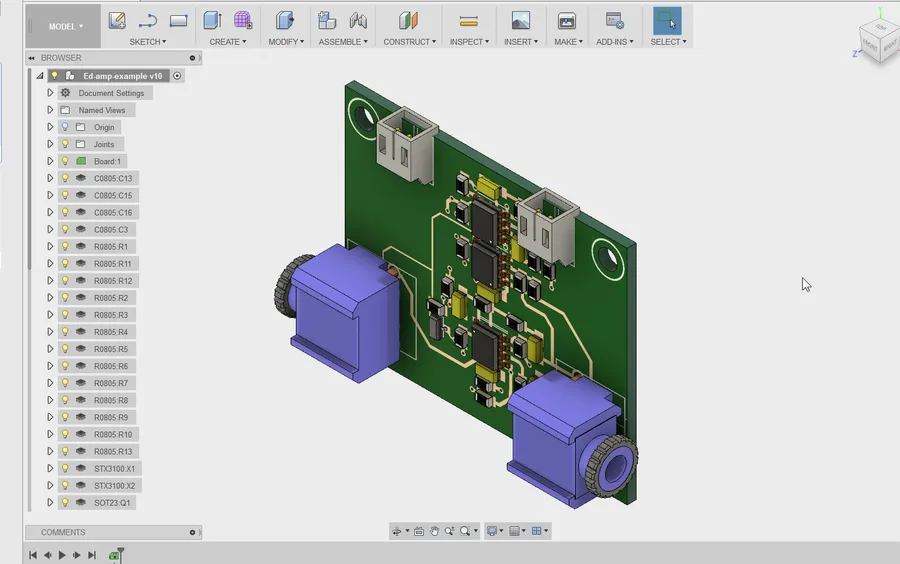
Optimizing PCB designs for JLCPCB's manufacturing process is crucial for ensuring successful production, minimizing errors, and reducing costs. Adhering to their specific design rules and capabilities is essential for a smooth transition from design to fabrication and assembly. This section outlines best practices and actionable insights to help you create PCBs that are perfectly suited for JLCPCB.
The PCB manufacturing industry is undergoing a rapid transformation, driven by technological advancements and evolving market demands. Companies like JLCPCB are not just participants but active drivers of innovation, shaping the future of how PCBs are designed, manufactured, and utilized across various sectors. This section explores these potential future trends and the impact on the industry.
Key trends and innovations that are likely to shape the future of PCB manufacturing, especially with companies like JLCPCB in the forefront, include:
JLCPCB's role in this evolving landscape includes leveraging its production capacity and technological prowess to adapt to these changes. Their potential evolution in key areas such as HDI, flexible PCB production, advanced material usage, and automated manufacturing processes are expected to solidify their place in the global market.
JLCPCB has revolutionized access to PCB manufacturing and assembly, making it easier than ever for engineers, hobbyists, and businesses to bring their electronic designs to life. By understanding their services, pricing, and best practices, you can effectively leverage JLCPCB for your next project. Whether you are prototyping a complex board or doing a small batch run for a personal project, JLCPCB offers a powerful and versatile solution. As the electronics landscape evolves, JLCPCB is likely to remain a key partner for many in the future. Remember to always double check your designs for optimal manufacturing when using jlc pcb.

