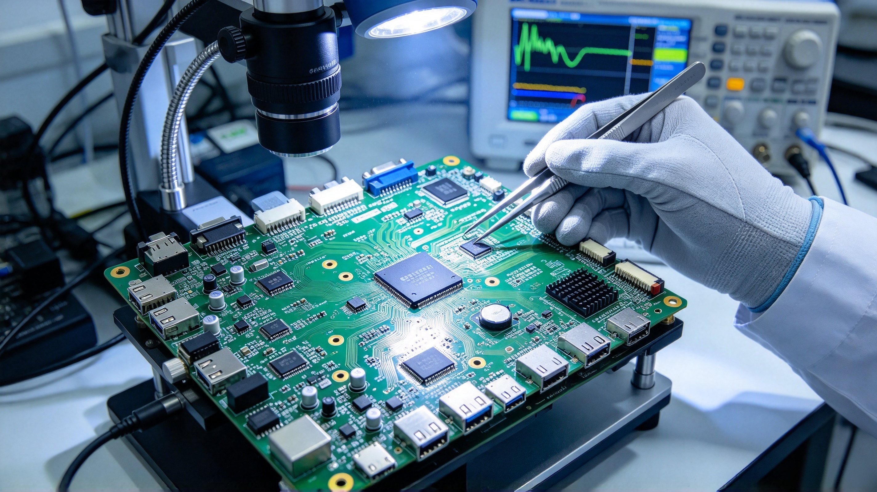
Introduction: Some PCB problems aren't caused by design errors—they're caused by physical effects. This guide covers 15 common PCB circuit effects, from bridging and ripple to crosstalk, reflection, thermal expansion, and via effects—explaining the symptoms, root causes, and mitigation measures for each.
Description: Based on AnyPCBA's small-to-medium volume PCB and PCBA manufacturing experience, this guide explains 15 common PCB circuit effects—their symptoms, causes, and mitigation measures—and how DFM review catches these physical risks before production.
In PCB design and manufacturing, some problems aren't caused by "drawing errors"—they're caused by physical effects. These effects don't show up in schematics or DRC checks, but they can cause signal distortion, interference, and even component failure in real operation.
This guide covers 15 common PCB circuit effects—symptoms, causes, and mitigation measures—with AnyPCBA's manufacturing perspective.
Symptom: In high-density routing, when there isn't enough space between two traces, one trace may appear suspended over another, resembling a bridge.
Impact: Can cause signal crosstalk, electromagnetic interference, and signal distortion or delay.
Mitigation:
Plan PCB layout carefully, keeping signal traces straight and avoiding crossings or overlaps
Optimize routing to maximize spacing between signal traces
Use layer stack-up design to place different signals on different layers
Plan signal and ground layers properly to reduce electromagnetic interference
Symptom: In high-speed circuits, when signal transmission speed is fast, signals may show ripple-shaped distortion as they propagate across the board.
Impact: Signal distortion, clock skew, crosstalk, and interference.
Mitigation:
Optimize layout and routing, minimizing bends, crossings, and branches
Use appropriate signal trace and ground designs to reduce crosstalk
Apply signal compensation or pre-emphasis techniques
Choose appropriate signal transmission lines and processing components
Symptom: Sudden voltage changes during signal transmission.
Impact: Components on the board may receive excessive voltage stress, damaging them or causing circuit failure.
Mitigation:
Optimize signal trace design for impedance matching and stability
Use appropriate power filters and decoupling capacitors to reduce source interference
Apply signal pre-emphasis or compensation techniques
Choose appropriate components and circuit protection devices
Symptom: Inductance, capacitance, and impedance parameters on the board can cause signal resonance at specific frequencies.
Impact: Affects stable signal transmission. When external signal frequency matches the circuit's natural frequency, resonance occurs.
Mitigation:
Optimize layout and design to avoid natural frequencies close to external excitation frequencies
Use compensation circuits or filters to suppress resonance
Choose appropriate damping components or materials
Apply appropriate circuit tuning techniques
Symptom: In high-speed circuits, due to electromagnetic radiation and other factors, signals may appear suspended on conductors or the board surface.
Impact: Affects signal transmission and reception.
Mitigation:
Optimize layout and design, planning signal trace routing and spacing carefully
Use appropriate signal trace and ground designs for impedance matching
Use shielding cans or shielding materials to reduce electromagnetic radiation
Choose appropriate board materials and components
Symptom: Due to dense signal trace layout or electromagnetic interference, signal crosstalk occurs between different traces.
Impact: Signal quality degradation or circuit malfunction.
Mitigation:
Optimize layout and design, planning trace routing and spacing carefully
Use shielding cans, shielding materials, or ground isolation
Use differential signal routing or add signal layers
Choose appropriate board materials and components
Symptom: In high-speed signal transmission, when signals encounter impedance mismatch or the receiving end doesn't fully absorb signal energy, signals reflect back to the source.
Impact: Signal waveform distortion, affecting transmission quality and stability.
Mitigation:
Design signal traces properly for impedance matching
Use termination resistors or capacitors to absorb signal energy
Optimize layout and design, shortening signal trace length
Choose appropriate board materials and components
Symptom: Metal layers or shielding cans on the PCB may shield signals.
Impact: Affects signal transmission range and quality.
Mitigation:
Design layout carefully, avoiding overlap or proximity between signal traces and shielding areas
Choose appropriate shielding materials with good shielding performance and minimal impact on signal transmission
Design appropriate grounding structures to reduce shielding effects
For signals that must pass through shielded areas, apply signal conditioning techniques
Symptom: Temperature changes can cause PCB material thermal expansion or contraction.
Impact: Affects board dimensional stability and component connection state.
Mitigation:
Choose PCB materials with lower thermal expansion coefficients
Avoid directly connecting high-CTE and low-CTE materials
Control soldering temperature and time to avoid solder joint cracking or component displacement
Add appropriate support structures in the PCB design
Symptom: When many ground vias exist on the board and they are close to signal traces or other ground vias, via effects may occur.
Impact: Affects signal transmission stability.
Mitigation:
Design appropriate via parameters—diameter, pitch, copper pad diameter—for impedance matching and consistency
Use via filling techniques to reduce via impact on signal transmission
Plan layout carefully to minimize via count and density
Choose appropriate layer stack-up to minimize vias between inner and outer layers
Symptom: Filling materials on the PCB may affect signal transmission—for example, different dielectric constants can change signal transmission speed or cause attenuation.
Mitigation:
Choose filling materials with dielectric constants close to the PCB material
Control filling material thickness to avoid lengthening the signal path and increasing attenuation
Optimize layout to minimize impact on signal transmission paths
Choose filling materials with lower resistance and dielectric loss
Symptom: Temperature changes on the PCB can cause material thermal expansion or contraction, affecting dimensional stability and component connection state.
Mitigation:
Choose PCB materials with good thermal and dimensional stability
Control soldering temperature and time to avoid component and joint damage
Plan layout carefully to reduce CTE differences between components
Control temperature changes in the PCB's operating environment
Symptom: Transistors and other components in PCB routing may be affected by the surrounding environment, causing parameter changes.
Impact: Affects circuit performance.
Mitigation:
Plan layout carefully to avoid external interference on transistors and other components
Control PCB operating temperature during design and manufacturing
Choose transistors and other components with good interference immunity and stability
Use compensation circuits to correct component parameter drift
Symptom: Some restricted areas on the PCB—edges, power areas—may limit signal transmission or routing.
Mitigation:
Plan layout carefully, avoiding placing sensitive signal traces or components near restricted areas
Apply electromagnetic shielding measures for restricted areas susceptible to interference
Optimize power supply design for power areas with instability or noise issues
Use fine routing techniques when routing in restricted areas
Symptom: Hidden issues or faults on the PCB may suddenly appear during later testing or use.
Impact: Unexpected board impact or damage.
Mitigation:
Strictly control quality at every stage of PCB production
Establish complete testing and inspection processes for comprehensive PCB testing
Choose high-reliability, stable components and materials
Perform regular maintenance on produced PCBs
As a factory focused on small-to-medium volume PCB and PCBA manufacturing, AnyPCBA has accumulated years of experience in controlling these circuit effects.
Our manufacturing capabilities cover 2 to 64 layers, including HDI, rigid-flex, and high-frequency hybrid. We hold ISO 13485 (medical) and IATF 16949 (automotive) certifications.
During DFM review and production control, we focus on:
Stack-up structure: whether it's symmetrical and whether it affects thermal expansion and via effects
Material selection: whether Dk/Df matches signal rates and whether it affects filling effect and temperature drift
Routing density: whether it may trigger bridging and crosstalk effects
Impedance control: whether it meets reflection suppression requirements
Grounding design: whether it affects shielding and via effects
Process control: whether soldering temperature, lamination parameters, and plating uniformity affect thermal expansion and latent defects
Our engineers help you anticipate these physical effects at the design stage, so your boards are not only drawable, but stable and reliable to produce.
If you're working on PCB design, or want to learn more about circuit effects, contact us through our website.




