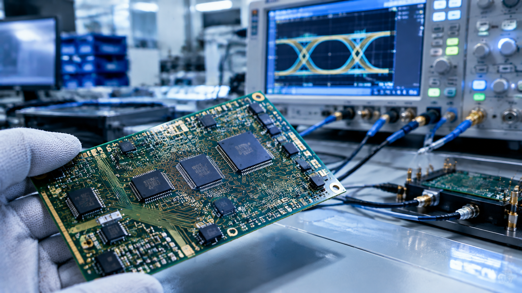
Introduction: Most PCBs carry some risk of signal integrity problems, especially in high-speed digital designs. This guide covers high-speed PCB design fundamentals—stack-up planning, impedance control, material selection, layout strategy, routing, and power integrity—from both an engineering and manufacturing perspective.
Description: Based on AnyPCBA's small-to-medium volume PCB and PCBA manufacturing experience, this guide explains high-speed PCB design from stack-up planning and impedance control to routing strategy and power integrity—and how DFM review catches manufacturability risks before production.
Most PCBs today carry some risk of signal integrity problems, typically related to high-speed digital design. High-speed PCB design focuses on creating boards that resist signal integrity (SI), power integrity (PI), and EMI/EMC issues. No design can avoid these problems entirely, but following high-speed design guidelines can reduce them to a negligible level.
This article covers the core elements of high-speed PCB design from both engineering and manufacturing perspectives.
High-speed design refers to systems using high-speed digital signals to transfer data between components. The general indicator for classifying a system as "high-speed" is the edge rate (or rise time) of the digital signals.
Most digital designs use both high-speed and low-speed protocols. In the embedded computing and IoT era, most high-speed boards also include an RF front-end for wireless communication.
While all designs start with a schematic, high-speed PCB design centers on interconnect design, stack-up design, and routing. If the first two are done well, the third is likely to succeed.
The stack-up determines impedance and routing difficulty. All stack-ups include layers dedicated to high-speed signals, power, and ground. Key considerations when allocating layers:
Board size and net count: larger boards may route all nets without multiple signal layers
Routing density: smaller boards force higher density, requiring more internal signal layers
Interface count: keeping all signals of one high-speed interface on the same layer ensures consistent impedance and skew
Low-speed and RF signals: these may consume surface space and require additional internal layers
Power integrity: large power and ground planes on adjacent layers provide high plane capacitance for stable decoupling
Before designing the stack-up, consider the layer count needed for all digital signals. Large high-speed ICs with BGA/LGA packages can also determine board size. During BGA fanout, each signal layer typically accommodates 2 rows—remember to include power and ground layers in the count.
Material selection:
As long as traces between components are not too long, FR4-grade materials are typically usable. If routing becomes too long, the channel will have excessive loss, and the receiver may not recover the signal.
The main material property to consider is the laminate's loss tangent. Lower loss tangent FR4 is a good starting point for smaller boards. For longer routing, more specialized materials may be needed—PTFE-based laminates, polarized glass laminates, or other special systems. For larger boards, Megtron or Duroid laminates are also good choices. Before proceeding, consult your manufacturer to ensure the material and stack-up are manufacturable.
Impedance can only be determined after creating a proposed stack-up and validating it with your manufacturer. The manufacturer may propose modifications—alternative materials or layer thicknesses. Once layer thicknesses are finalized, you can calculate impedance values.
Impedance is typically calculated using formulas or field solver tools. The required impedance determines transmission line dimensions and distance to nearby power or ground layers.
Tools for determining transmission line width:
IPC-2141 and Wadell formulas: a starting point for impedance estimation, accurate at lower frequencies
2D/3D field solvers: solve Maxwell's equations within the defined geometry
Using a layer stack manager with a field solver provides the most accurate results, accounting for copper roughness, etching, asymmetric trace arrangement, and differential pairs.
Most high-speed protocols (PCIe, Ethernet) use differential pairs, so trace width and spacing must be calculated for specific differential impedance. Field solvers are the best tool for any geometry (microstrip, stripline, or coplanar).
There are no fixed rules for component placement in high-speed layout. In general, placing the largest central processor IC near the board center is a good idea, since it connects to all other components.
Smaller ICs connected directly to the central processor can be placed around it, keeping routing short and direct. Peripheral devices go around the board. High-speed layout works best when the main controller is near the center, with high-speed peripherals around it.
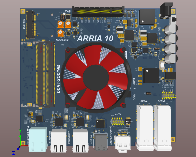 High-speed layout example: the central processor sits in the middle, with DDR4, PCIe, Ethernet, and USB peripherals arranged around it for short, direct routing.
At the detail level, the BGA fanout around the central processor determines how signals escape to inner layers. The density of via arrays and the routing channels between them directly affect impedance control and signal integrity.
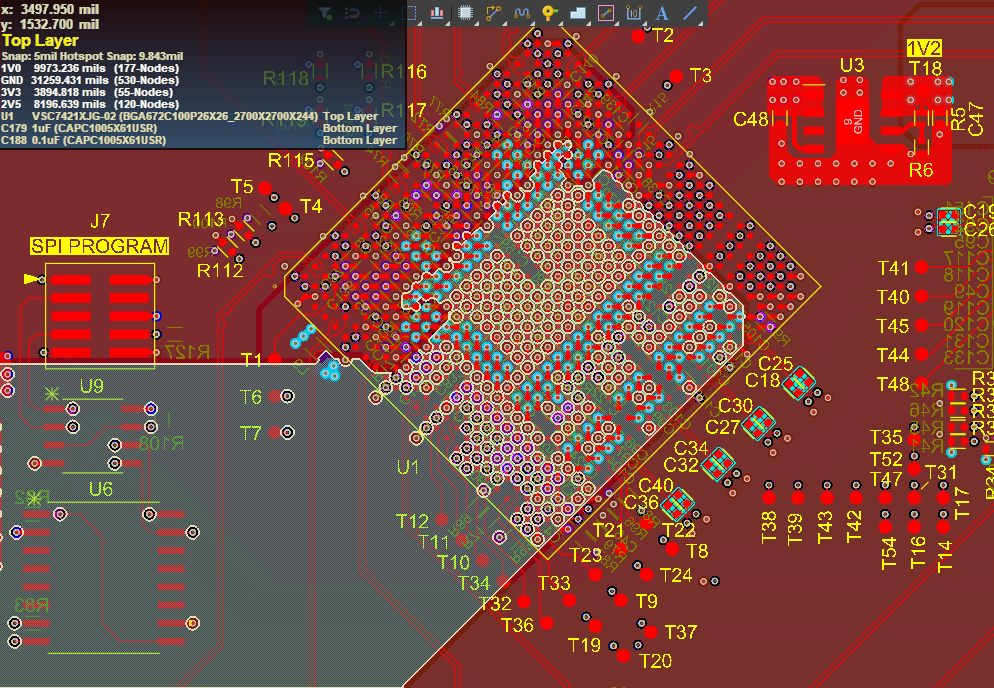
BGA fanout and routing in a high-speed PCB layout—dense via arrays and controlled-impedance traces around the central processor.
Signal integrity starts with designing specific impedance values and maintaining them during layout and routing. Other strategies include:
Shortening paths between components
Minimizing routing through vias—ideally only two vias to enter and exit inner layers
Eliminating short stubs on ultra-high-speed traces (10G+ Ethernet) through back drilling
Checking whether termination resistors are needed to prevent reflection
Consulting your manufacturer about materials and processes that avoid fiber weave effect
Using crosstalk calculations or simulation to determine appropriate net spacing
Keeping a list of buses and nets requiring length matching to eliminate skew
These points can be set as design rules in the routing tool.
Design rules ensure impedance, spacing, and length targets are met during routing. Important differential pair rules—minimizing length mismatch and enforcing spacing—ensure differential impedance targets are met.
Length tuning between traces in parallel buses and differential pairs ensures delay matching and eliminates skew at the receiver.
One of the most important points in high-speed routing is placing ground planes near traces. The stack-up should have ground planes adjacent to impedance-controlled signals, maintaining consistent impedance and clear return paths. Traces should not cross gaps or cracks in ground layers, avoiding impedance discontinuities that cause EMI. Ground planes also support power integrity and stable power delivery.
Power integrity is highly relevant to high-speed PCB design. Ensuring stable power to high-speed components is critical—power integrity problems can masquerade as signal integrity problems.
The PCB stack-up and PDN layout are the main factors determining power integrity. Done well, power is delivered with low noise and minimal transient oscillation on the power rail. High-speed PCBs with good power integrity ensure low emissions, low-noise power delivery, and eliminate some SI problems.
As a factory focused on small-to-medium volume PCB and PCBA manufacturing, AnyPCBA has accumulated years of experience in high-speed PCB manufacturing.
Our manufacturing capabilities cover 2 to 64 layers, including HDI, rigid-flex, and high-frequency hybrid. We hold ISO 13485 (medical) and IATF 16949 (automotive) certifications.
For high-speed PCB projects, we support:
Stack-up structure review: evaluating stack-up feasibility based on impedance requirements and routing density, including dielectric thickness, copper thickness, and material selection
Impedance control support: assisting with impedance calculations based on stack-up and materials, and verifying impedance consistency through TDR testing in production
Material availability confirmation: for high-speed materials (low-loss FR4, PTFE, Megtron), confirming lead times and availability during DFM review to avoid delays
Back drilling support: for 10G+ high-speed signals, eliminating via stub effects on signal integrity
Surface treatment selection: providing ENIG, immersion silver, immersion tin, and other options based on high-speed requirements
DFM review: checking stack-up design, via processes, impedance control, and material selection for manufacturability before project launch
Our engineers help you confirm these critical details at the design stage, so your high-speed boards are not only drawable, but stable and reliable to produce.
If you're working on high-speed PCB design, or want to learn more about our manufacturing capabilities, contact us through our website.
What challenges have you encountered in high-speed PCB design? Share your experience in the comments.




