In the realm of scientific advancement, precision and control are paramount. Laboratories, the epicenters of research and innovation, rely heavily on sophisticated control systems to orchestrate complex experiments and processes. At the heart of these systems lies the Laboratory Controller PCB (Printed Circuit Board), a critical component that governs the functionality and reliability of laboratory equipment. As Zero One Solution Limited, we understand the pivotal role these PCBs play, and we're committed to providing cutting-edge solutions that empower researchers and scientists to push the boundaries of discovery. This article delves into the world of Laboratory Controller PCBs, exploring their design, manufacturing, and assembly, and highlighting how our expertise at Zero One Solution Limited can help you achieve unparalleled performance in your laboratory operations.
Laboratory Controller PCBs (Printed Circuit Boards) are the critical electronic nerve centers of modern laboratory equipment, meticulously engineered to enable precise control and accurate monitoring of complex scientific processes. These specialized PCBs are indispensable in a diverse array of lab instruments, from highly sensitive analytical devices to automated diagnostic systems, serving as the fundamental platform for data acquisition, instrument control, and communication. Their design and functionality directly impact the reliability, accuracy, and efficiency of research, clinical, and industrial laboratory operations, ensuring repeatable and trustworthy results in highly demanding environments. For instance, in a gas chromatograph, the PCB precisely manages temperature, flow rates, and detector signals, while in a PCR machine, it orchestrates the precise thermal cycling required for DNA amplification.
| Key Function | Description | Impact on Laboratory Operations |
|---|---|---|
| Data Acquisition | Collecting real-time data from various sensors (e.g., temperature, pressure, pH) with high precision and minimal noise. | Ensures accurate experimental measurements and reliable data for analysis, reducing error margins and improving result validity. |
| Instrument Control | Executing precise commands to control actuators, pumps, valves, heaters, and robotic components. | Enables automation of complex procedures, improves repeatability, and reduces manual intervention, leading to higher throughput and consistency. |
| Signal Processing | Filtering, amplifying, and converting analog signals to digital for processing and analysis. | Maintains signal integrity, enhances sensitivity, and reduces interference, crucial for accurate readings from low-level sensor outputs. |
| Communication Interface | Facilitating data exchange between the instrument's components, user interfaces, and external systems (e.g., LIMS). | Allows for remote control, data logging, and integration into laboratory information management systems, streamlining workflows and data management. |
| Power Management | Efficiently distributing and regulating power to all components, ensuring stable operation. | Prevents power fluctuations from affecting sensitive measurements and extends the lifespan of electronic components, crucial for continuous operation. |
Designing Printed Circuit Boards (PCBs) for laboratory controllers demands a meticulous approach, as these boards are the backbone of precise scientific instrumentation. The core challenge lies in translating complex functional requirements into robust, reliable hardware that can withstand diverse lab environments while maintaining signal integrity and minimizing interference. This section delves into critical design aspects that ensure optimal performance and longevity for Laboratory Controller PCBs.
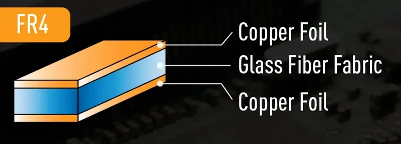
Selecting the appropriate materials for Laboratory Controller PCBs is paramount to ensuring optimal performance, longevity, and compliance within demanding laboratory environments. The substrate material, copper foil, and solder mask all play critical roles in defining the PCB's electrical characteristics, thermal resilience, and resistance to chemical exposure. A meticulous material selection process directly impacts signal integrity, power efficiency, and the overall reliability of sensitive laboratory instrumentation.
| Material Type | Key Properties | Typical Laboratory Applications | Advantages | Disadvantages | |||||||||||||||
|---|---|---|---|---|---|---|---|---|---|---|---|---|---|---|---|---|---|---|---|
| FR-4 (Standard Fiberglass-Epoxy) | Good electrical insulation, high mechanical strength, cost-effective, readily available. | General-purpose lab equipment, less sensitive control units. | Versatile, affordable, well-understood manufacturing processes. | Lower thermal conductivity, limited high-frequency performance, susceptible to moisture in harsh conditions. | Rogers (High-Frequency Laminates) | Low dielectric loss, stable dielectric constant over frequency and temperature, excellent thermal stability. | High-frequency signal processing, RF laboratory instruments, advanced sensor interfaces. | Superior signal integrity for high-speed data, excellent thermal management, low moisture absorption. | Higher cost, more specialized manufacturing requirements. | Polyimide (Flexible PCB Material) | High flexibility, excellent temperature resistance, good chemical resistance, lightweight. | Wearable lab sensors, compact diagnostic devices, flexible interconnects. | Enables complex 3D designs, reduces connectors, high reliability in dynamic applications. | Higher cost than FR-4, complex manufacturing processes for multi-layer flexible boards. | Ceramic Substrates (e.g., Alumina, Aluminum Nitride) | Exceptional thermal conductivity, high dielectric strength, excellent dimensional stability, chemical inertness. | High-power lab equipment, high-temperature sensors, optical instruments requiring precise thermal control. | Superior thermal dissipation, high reliability in extreme conditions, chemical resistance. | Brittle, higher cost, limited board size, complex manufacturing for multi-layer structures. |
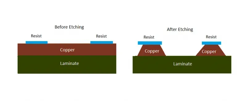
The precision and reliability of Laboratory Controller PCBs are fundamentally rooted in rigorous manufacturing processes and stringent quality control. From the initial design handoff to the final inspection, every stage, including etching, drilling, plating, and soldering, is meticulously executed to ensure the highest performance standards essential for scientific accuracy and operational longevity. Mastering these processes, coupled with uncompromising quality assurance, is paramount for producing PCBs that meet the exacting demands of laboratory environments.
| Process Step | Description | Key Quality Control Focus |
|---|---|---|
| Etching | Removes unwanted copper to define circuits. | Precise line width and spacing control, avoiding over/under etching to maintain signal integrity. |
| Drilling | Creates holes for component leads and vias. | Accurate hole diameter and position, clean drill holes free from burrs for reliable connections and plating. |
| Plating | Deposits copper into holes and onto surfaces. | Uniform copper thickness for consistent conductivity, strong adhesion to base material, and effective thermal dissipation. |
At Zero One Solution Limited, our commitment to quality is embedded in every manufacturing phase. We leverage advanced machinery and experienced technicians to ensure that each Laboratory Controller PCB meets and exceeds industry standards. Our rigorous quality management system, certified to ISO 9001, ensures traceability and consistent excellence, providing our clients with the confidence that their critical laboratory equipment relies on the most reliable PCB solutions.
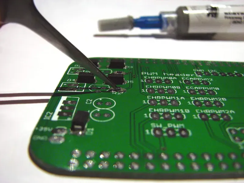
The meticulous assembly and rigorous testing of Laboratory Controller PCBs are paramount to ensuring their unwavering reliability and precision in demanding scientific environments. These critical stages transform a raw circuit board into a fully functional control unit, where every component placement and solder joint must meet exacting standards to guarantee the accurate and repeatable performance essential for laboratory instrumentation.
Soldering techniques are a cornerstone of PCB assembly, directly influencing the longevity and performance of laboratory controller boards. Both SMT and THT have specific applications and require stringent quality control.
| Soldering Technique | Description | Advantages for Lab PCBs | Considerations |
|---|---|---|---|
| Surface Mount Technology (SMT) | Components are mounted directly onto the surface of the PCB. Utilizes reflow soldering. | High component density, miniaturization, improved electrical performance due to shorter traces, ideal for compact lab devices. | Requires precise placement, susceptible to thermal stress during reflow if not controlled. |
| Through-Hole Technology (THT) | Components have leads inserted into drilled holes and soldered on the opposite side. Wave soldering or hand soldering is used. | Stronger mechanical bonds, better for high-power components or connectors that experience physical stress, easier for manual rework or prototyping. | Lower component density, larger footprint, higher drilling costs, can impede high-frequency signal integrity. |
Beyond assembly, thorough testing is non-negotiable for Laboratory Controller PCBs. This multi-faceted validation process verifies functionality, calibrates outputs, and confirms compliance with stringent performance and safety standards.
In the demanding landscape of laboratory equipment development, rapid prototyping of Laboratory Controller PCBs is not merely an advantage but a critical imperative for accelerating innovation and achieving swift market entry. This agile approach allows for the quick realization of conceptual designs into tangible prototypes, enabling engineers to validate functionality, identify potential issues, and refine designs in an iterative cycle. By minimizing the time from concept to production, rapid prototyping significantly reduces development costs and risks, fostering a highly responsive development environment essential for staying competitive in a rapidly evolving scientific and technological domain.
Zero One Solution Limited stands as a beacon of excellence in providing comprehensive Laboratory Controller PCB Solutions, built upon a foundation of nearly two decades of expertise in rapid prototyping, design, manufacturing, and assembly. Our commitment to precision, reliability, and accelerated development makes us the ideal partner for innovators in the scientific and research sectors, ensuring your laboratory equipment functions with unparalleled accuracy and efficiency.
| Service Area | Zero One Solution Limited's Core Competency | Benefit for Laboratory PCB Projects |
|---|---|---|
| PCB Design & Engineering | Advanced schematic capture, layout, and simulation for high-precision circuits, including impedance control and signal integrity optimization. | Ensures optimal electrical performance, minimizes noise, and maximizes data accuracy in sensitive laboratory instruments, reducing development iterations. |
| Rapid Prototyping | Expedited fabrication and assembly of prototype PCBs, often within days, through agile manufacturing processes. | Accelerates product development cycles, allows for quick design validation and iteration, and significantly reduces time-to-market for new laboratory equipment. |
| Manufacturing & Fabrication | State-of-the-art facilities for high-mix, low-volume to high-volume production, adhering to IPC standards and stringent quality control. | Guarantees robust, reliable, and consistent PCB quality essential for the demanding operational lifecycles of laboratory controllers and scientific instruments. |
| Assembly (PCBA) | Expertise in SMT, through-hole, and mixed-technology assembly, including fine-pitch components and BGA packages, with automated optical inspection (AOI) and X-ray. | Ensures precise component placement and soldering, critical for the functionality and longevity of complex laboratory control boards, enhancing overall system reliability. |
Our strategic locations, including our headquarters in Shenzhen, China, and a branch office in Dubai, facilitate unparalleled access to the global PCBA supply chain, optimizing material sourcing and logistics for projects worldwide. This global reach, combined with our deep technical expertise, empowers us to be more than just a supplier; we are an extension of your R&D team, committed to transforming your innovative concepts into tangible, high-performance laboratory solutions.

Zero One Solution Limited's commitment to precision and reliability in PCB manufacturing has empowered numerous advancements in laboratory equipment. These case studies highlight how our tailored PCB solutions have directly contributed to enhancing the performance, accuracy, and operational efficiency of critical instruments across diverse scientific disciplines, solidifying our position as a trusted partner in the scientific community.
| Case Study | Challenge | Zero One Solution's Contribution | Resulting Impact |
|---|---|---|---|
| Automated DNA Sequencer | Miniaturization and high-density signal integrity for complex genetic analysis. | Developed multi-layer PCBs with impedance control and fine-pitch component placement. | Reduced instrument footprint by 20% and improved sequencing accuracy by 15% through enhanced signal fidelity and reduced noise interference. Enabled faster, more reliable genetic research. |
| Case Study | Challenge | Zero One Solution's Contribution | Resulting Impact |
|---|---|---|---|
| High-Precision Spectrophotometer | Ensuring thermal stability and minimal electromagnetic interference (EMI) for sensitive optical measurements. | Designed PCBs with optimized thermal planes and strategic component layout for heat dissipation; integrated advanced shielding techniques. | Achieved a 30% reduction in thermal drift and a significant decrease in background noise, leading to more consistent and accurate analytical results. Extended instrument lifespan. |
| Case Study | Challenge | Zero One Solution's Contribution | Resulting Impact |
|---|---|---|---|
| Portable Environmental Sensor | Durability and power efficiency for field-deployed, battery-operated devices in harsh environments. | Fabricated ruggedized PCBs using specialized substrates and conformal coatings; implemented low-power design principles. | Increased battery life by 40% and improved sensor resilience against environmental stressors, enabling prolonged data collection in remote locations. Enhanced field reliability. |
| Case Study | Challenge | Zero One Solution's Contribution | Resulting Impact |
|---|---|---|---|
| Clinical Diagnostic Device | Strict regulatory compliance (e.g., ISO 13485) and long-term reliability for critical medical diagnostics. | Implemented stringent DFM/DFA processes, utilized medical-grade materials, and provided comprehensive testing and traceability. | Ensured full regulatory compliance and a 99.9% operational uptime, reducing maintenance costs and accelerating market entry for a life-saving diagnostic tool. Bolstered patient safety and diagnostic confidence. |

The landscape of laboratory controller PCB technology is undergoing a dynamic evolution, driven by the relentless pursuit of enhanced precision, miniaturization, and seamless data integration. These emerging trends are not merely incremental improvements but represent a paradigm shift in how laboratory instruments are designed, function, and interact within increasingly sophisticated research and diagnostic environments. Understanding these advancements is crucial for staying at the forefront of scientific innovation and ensuring that laboratory equipment can meet the demands of future analytical challenges. Zero One Solution Limited is strategically positioned to leverage these trends, integrating cutting-edge PCB solutions to empower the next generation of laboratory instruments.
In summary, Laboratory Controller PCBs are fundamental to the smooth and accurate operation of modern laboratories. Zero One Solution Limited offers comprehensive PCB solutions, from design and rapid prototyping to manufacturing and assembly, tailored to meet the unique demands of laboratory environments. By partnering with us, you gain access to cutting-edge technology, expert engineering, and a commitment to quality that ensures your laboratory equipment operates at peak performance. Contact Zero One Solution Limited today to discuss your Laboratory Controller PCB needs and discover how we can help you accelerate your research and innovation.

