In today's rapidly evolving technological landscape, STEM (Science, Technology, Engineering, and Mathematics) education is more critical than ever. Equipping students with hands-on experience is paramount, and printed circuit boards (PCBs) serve as the foundational building blocks for countless electronic projects. Zero One Solution Limited provides specialized PCB solutions tailored for STEM education development boards, enabling educators and students to bring their innovative ideas to life. But how exactly do high-quality PCBs contribute to a more effective STEM learning environment? This article explores the crucial role of PCB solutions in STEM education, highlighting how Zero One Solution Limited is empowering the next generation of innovators.
Introduction to STEM Education and the Role of PCBs
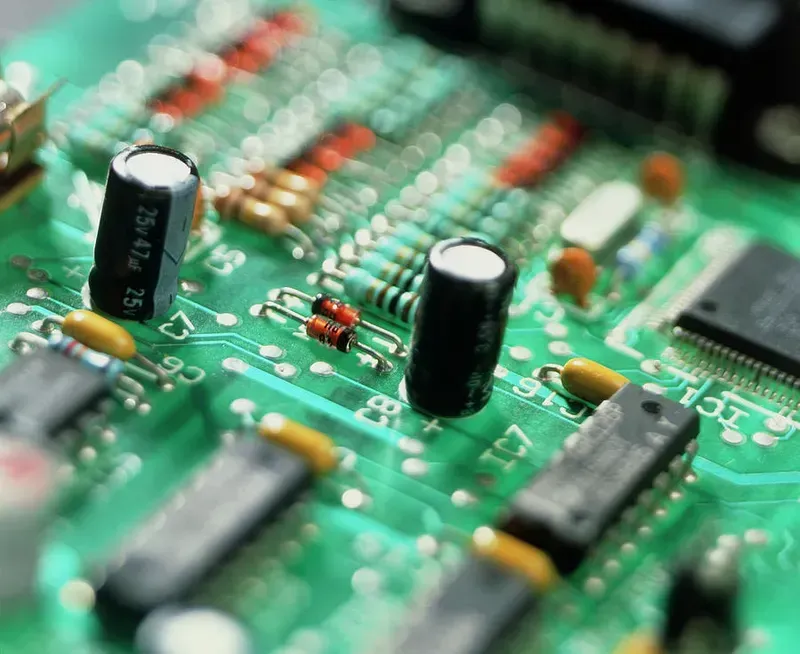
PCB Circuit Board Close-Up
In the rapidly evolving landscape of the 21st century, STEM (Science, Technology, Engineering, and Mathematics) education stands as the cornerstone for fostering critical thinking, innovation, and problem-solving skills essential for future generations. It transcends traditional disciplinary boundaries, promoting an integrated approach to learning that prepares students for careers in burgeoning fields. At the heart of practical STEM learning, particularly in electronics and robotics, lies the Printed Circuit Board (PCB). These fundamental components are the unseen backbone of virtually all electronic devices, serving as the physical foundation upon which circuits are built, enabling the tangible application of theoretical STEM concepts into real-world, functional prototypes.
What is STEM Education? STEM education is an interdisciplinary approach to learning that removes the traditional barriers separating the four disciplines—science, technology, engineering, and mathematics—and integrates them into a cohesive learning paradigm. Its goal is to prepare students for the demands of the modern workforce by equipping them with critical thinking, problem-solving, and innovation skills.
Why is STEM Education important for 21st-century learners? STEM education is crucial for 21st-century learners because it addresses the increasing demand for a skilled workforce in technology-driven industries. It fosters creativity, encourages collaboration, and develops analytical abilities, empowering students to tackle complex global challenges and drive innovation across various sectors.
How do PCBs integrate into STEM learning? PCBs are integral to STEM learning as they provide a practical platform for students to apply theoretical knowledge in electronics and engineering. By designing, manufacturing, and assembling PCBs, students gain hands-on experience with circuit design, component integration, and system functionality, bridging the gap between abstract concepts and tangible results.
What specific STEM fields benefit most from PCB-centric learning? Electronics, robotics, computer science, and mechatronics are among the STEM fields that benefit most from PCB-centric learning. These disciplines rely heavily on the physical implementation of circuits and systems, making hands-on PCB experience invaluable for understanding device functionality, prototyping new designs, and troubleshooting complex electronic systems.
What role does PCB rapid prototyping play in accelerating STEM education? PCB rapid prototyping significantly accelerates STEM education by allowing students and educators to quickly iterate on designs, test hypotheses, and validate concepts. This agile approach minimizes development cycles, reduces costs associated with errors, and provides immediate feedback, thereby enhancing the learning process and fostering a culture of continuous experimentation and improvement.
Challenges in STEM Education Development Board PCB Design
Designing and producing Printed Circuit Boards (PCBs) for STEM education development boards presents a unique set of challenges that can hinder hands-on learning and project development. These hurdles often revolve around the inherent complexity of electronic design, the significant costs associated with prototyping and manufacturing, and the critical time constraints faced by both educators and students in project timelines. Overcoming these obstacles is paramount to fostering effective and engaging STEM learning experiences.
Complexity of PCB Design for STEM Projects For students and educators, the intricate nature of PCB design, including schematic capture, layout, routing, and component selection, can be overwhelming. The learning curve for sophisticated design software is steep, and ensuring signal integrity, power distribution, and thermal management for educational projects requires specialized knowledge often beyond the scope of introductory STEM curricula. This complexity can deter beginners and slow down project progression.
Cost Constraints in Educational Budgets Educational institutions and individual students often operate under strict budget limitations. The cost of materials, fabrication, and assembly for even simple PCBs can quickly accumulate, especially when multiple iterations are needed. This financial barrier can limit the number and complexity of projects undertaken, impacting the accessibility and scalability of hands-on STEM learning experiences. High-quality rapid prototyping services become essential to mitigate these costs.
Time Constraints for Project Completion STEM projects in educational settings are typically bound by academic calendars and deadlines. Traditional PCB manufacturing processes can involve lengthy lead times, from design finalization to fabrication and delivery. This extended timeline directly impacts the ability of students to iterate on their designs, test prototypes, and complete projects within the allotted timeframes, potentially leading to rushed work, reduced learning outcomes, and frustration. Rapid turnaround times for PCB production are crucial for agile educational development.
Zero One Solution's Comprehensive PCB Solutions for STEM
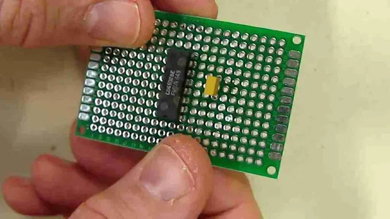
PCB Prototype Sample
Zero One Solution Limited stands at the forefront of providing comprehensive Printed Circuit Board (PCB) solutions specifically tailored for STEM education development boards. Our expertise, honed since 2011, lies in transforming innovative educational concepts into tangible, high-quality PCBs. We understand the critical need for reliable, efficient, and accessible PCB services in fostering the next generation of engineers and innovators. Our one-stop service model, from rapid prototyping to full-scale manufacturing and assembly, streamlines the development process for educational institutions and individual learners, ensuring that complex electronic projects are not only feasible but also highly effective for hands-on learning experiences.
Rapid Prototyping for Iterative Learning Zero One Solution excels in rapid prototyping, enabling educators and students to quickly iterate on their PCB designs. This accelerated process is crucial in STEM education, allowing for real-time testing, immediate feedback, and rapid design improvements, significantly shortening project cycles and enhancing learning outcomes.
One-Stop PCB Services from Design to Assembly We offer an end-to-end solution that encompasses every stage of PCB development. From initial design consultation and optimization for manufacturability (DFM) to high-precision manufacturing and efficient assembly (PCBA), Zero One Solution simplifies the entire process. This integrated approach ensures seamless transitions between stages, reduces logistical complexities, and guarantees consistent quality for educational development boards.
Specialized Expertise in Educational Board Requirements Understanding the unique demands of STEM education, Zero One Solution focuses on durability, safety, and ease of use in our PCB solutions. We ensure that development boards are robust enough for repeated handling in classroom settings and are designed with clear labeling and user-friendly interfaces to facilitate effective learning.
Service Area
Key Offering for STEM Education
Benefit to STEM Programs
PCB Design & Layout
Optimized designs for educational projects, DFM services
Ensures robust, functional, and easily manufacturable boards, reducing design errors and costs for students and educators
Rapid PCB Prototyping
Quick-turn fabrication for small batches
Accelerates experimentation and iteration, allowing for faster learning cycles and project development
PCB Manufacturing
High-quality fabrication (2-32 layers)
Provides durable and reliable boards capable of supporting diverse educational applications, from robotics to IoT
Component Sourcing & Kitting
Access to global component network, kitting services
Simplifies bill of materials (BOM) management and assembly for educational labs, ensuring correct components are readily available
PCBA (Assembly)
Automated SMT & THT assembly, rigorous quality control
Delivers fully assembled boards, ready for immediate use, saving valuable time and resources in educational settings
Rapid Prototyping for Accelerated Learning
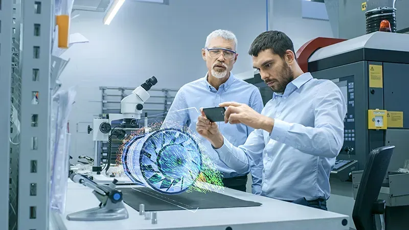
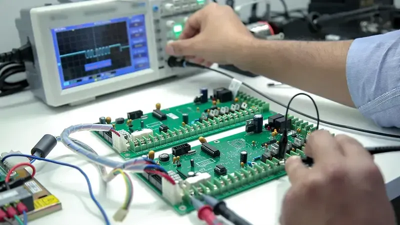
Engineer Working on Prototype
Rapid prototyping stands as a cornerstone in accelerating learning within STEM education, transforming theoretical concepts into tangible, testable realities. This iterative process, vital for product development, enables students to quickly validate designs, identify flaws, and refine their projects, fostering an agile mindset critical for future innovation. Zero One Solution Limited champions this approach, providing rapid-response PCB prototyping services that significantly compress the design-to-testing cycle for educational development boards, thereby enhancing the practical learning experience and empowering students to innovate with speed and confidence.
Reduced Iteration Time Traditional PCB manufacturing can involve lengthy lead times, stifling the dynamic nature of STEM projects. Our rapid prototyping capabilities drastically reduce these cycles, often delivering functional boards within days, allowing students to test, learn, and re-design without significant delays. This efficiency keeps projects engaging and maintains momentum in the learning process.
Enhanced Hands-on Experience Direct interaction with physical prototypes deepens understanding far beyond theoretical instruction. Rapid prototyping provides students with immediate access to their designs in a physical form, enabling them to troubleshoot, debug, and observe the real-world performance of their circuits, reinforcing foundational electrical engineering and computer science principles.
Fostering Innovation and Experimentation The ability to quickly prototype encourages a culture of experimentation. Students are more inclined to try unconventional designs or complex functionalities when the barrier to creating a physical model is low. This freedom to iterate and experiment is crucial for nurturing creative problem-solving and innovative thinking, preparing them for real-world engineering challenges.
PCB Design and Manufacturing Expertise
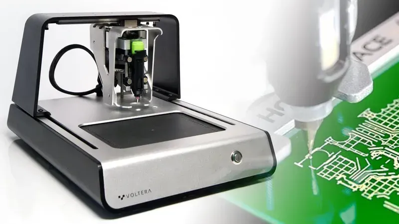
PCB Manufacturing Equipment
At the core of robust STEM education development boards lies exceptional PCB design and manufacturing. Zero One Solution Limited offers unparalleled expertise in bringing these critical components to life, ensuring every board functions reliably under the rigorous demands of educational projects and rapid prototyping. Our comprehensive capabilities span the entire PCB lifecycle, from initial design consultation to high-precision fabrication and assembly, specifically tailored to support innovative learning environments and accelerate product development for aspiring engineers.
Advanced Design Methodologies Our engineers leverage cutting-edge CAD software and simulation tools to create optimized PCB layouts. We focus on design for manufacturability (DFM) and design for assembly (DFA) to prevent common issues like signal integrity problems, power delivery network instability, and thermal management challenges. For STEM education boards, this translates to designs that are not only functional but also resilient and user-friendly for learners.
High-Precision Manufacturing Processes Zero One Solution employs state-of-the-art manufacturing facilities, adhering to international quality standards such as IPC-A-600. Our processes include precise drilling, advanced plating techniques, and meticulous solder mask application, ensuring high-yield production of durable PCBs. This precision is vital for educational boards where consistency and reliability are paramount for accurate experimentation and long-term use.
Component Sourcing and Assembly Excellence Beyond bare board fabrication, we offer comprehensive component sourcing and PCBA services. Our global supply chain network ensures access to a wide range of components, from basic resistors and capacitors to complex microcontrollers, at competitive prices. Our automated SMT (Surface Mount Technology) and THT (Through-Hole Technology) assembly lines guarantee precise component placement and robust soldering, minimizing defects and maximizing operational longevity, crucial for educational institutions operating on limited budgets and resources.
Rigorous Quality Assurance Every PCB undergoes stringent quality control checks, including Automated Optical Inspection (AOI), X-ray inspection for complex assemblies, and functional testing. This multi-stage verification process ensures that each development board meets specified performance criteria and is free from manufacturing defects, providing educators and students with reliable tools for their STEM endeavors.
Capability
Description
Benefit for STEM Education
Multi-Layer PCB Production
Ability to produce boards from 2 to 32 layers for complex circuit integration.
Enables creation of sophisticated, compact development boards for advanced projects.
High-Density Interconnect (HDI)
Advanced routing techniques for miniaturization and enhanced performance.
Supports smaller form factors for portable educational kits and integration into robotics.
Variety of Substrate Materials
Expertise in FR-4, high-Tg, and specialty laminates.
Allows customization for specific environmental or performance requirements, e.g., high-temperature applications.
Surface Finish Options
ENIG, HASL, OSP for optimal solderability and shelf life.
Ensures reliable connections for easy rework and long-term durability in student use.
Prototyping & Mass Production
Seamless scalability from single prototypes to large-volume orders.
Supports individual student projects and large-scale curriculum deployments.
Cost-Effective Solutions for Educational Budgets
For educational institutions and programs, budget constraints are a perennial concern, yet providing high-quality, reliable components for STEM education is paramount. Zero One Solution understands this critical balance, offering competitively priced PCB solutions that empower schools and universities to implement cutting-edge hands-on learning experiences without compromising on the quality and performance essential for educational development boards. Our streamlined processes and strategic global supply chain network enable us to deliver cost efficiencies directly to our clients, ensuring that financial limitations do not hinder innovation in STEM.
Aspect
Educational Budget Priority
Zero One Solution's Approach
Component Cost
Minimize individual part expenses
Volume discounts, optimized material sourcing, and efficient production to lower per-unit costs
Manufacturing Efficiency
Reduce overall project expenditure
Automated processes, rapid prototyping to minimize iterative costs, and optimized lead times
Quality Assurance
Ensure reliability and reduce reworks
Rigorous quality control, industry-standard compliance, and robust testing to prevent costly failures
Design Support
Access expert guidance without high consulting fees
Collaborative design review and DFM (Design for Manufacturability) support to prevent errors and reduce rework costs
Scalability
Ability to scale projects without disproportionate cost increases
Flexible production capacities from prototypes to small-batch runs, accommodating varying educational program sizes
How does Zero One Solution achieve cost-effectiveness without sacrificing quality for STEM Education Development Boards? Zero One Solution achieves cost-effectiveness through a multi-faceted approach. We leverage our extensive network for bulk material procurement, optimize our manufacturing processes for efficiency, and utilize advanced automation. Simultaneously, we maintain stringent quality control measures at every stage, from design verification (DFM) to final testing, ensuring that cost savings do not come at the expense of reliability or performance, which is crucial for educational tools that need to withstand repeated use and experimentation.
Case Studies: Successful STEM Projects with Zero One Solution PCBs
Students Using PCBs
Zero One Solution Limited consistently empowers innovation in STEM education by providing high-quality, reliable, and rapidly prototyped PCBs. Our commitment to excellence translates into tangible success stories, enabling students and educators to transform theoretical concepts into functional, impactful projects. These case studies highlight our role in accelerating learning and fostering creativity within the academic sphere.
Interactive Robotics Kit for High Schoolers A high school robotics club aimed to develop an interactive robot that could respond to voice commands. Zero One Solution provided rapid prototyping services for their custom-designed motor control and sensor integration PCBs. Our quick turnaround allowed the students to iterate on their designs multiple times within a single semester, leading to a robust and highly functional robot that won regional competitions. The students gained invaluable hands-on experience in circuit design, troubleshooting, and agile development methodologies.
Environmental Monitoring System for University Research A university research team required compact and durable PCBs for a network of environmental sensors deployed in remote locations. Zero One Solution delivered high-precision PCBs, ensuring signal integrity and power efficiency for their long-term data collection efforts. Our manufacturing expertise contributed to the reliability of the system, enabling the researchers to accurately monitor temperature, humidity, and air quality, leading to significant findings published in an academic journal. The project demonstrated the critical role of custom PCB solutions in advanced scientific research.
Benefits of Choosing Zero One Solution for STEM Education PCBs
Choosing the right partner for STEM education development board PCBs is critical to fostering innovation and practical learning. Zero One Solution Limited stands as a premier choice, offering a comprehensive suite of advantages that directly address the needs of educational institutions and aspiring engineers, ensuring high-quality, efficient, and cost-effective solutions that accelerate the learning curve and project success.
Rapid Prototyping and Fast Turnaround Our core strength lies in rapid-response R&D prototype manufacturing. This capability translates directly into faster project cycles for STEM programs, allowing students and educators to quickly iterate on designs, test hypotheses, and bring their ideas to fruition without significant delays. This agility is paramount in an educational setting where time-to-market (or rather, time-to-learning) is crucial for maintaining engagement and momentum.
One-Stop Integrated Services Zero One Solution provides end-to-end services, from initial PCB design and layout to manufacturing and final assembly. This integrated approach simplifies the procurement process for educational institutions, reduces coordination overhead, and minimizes the potential for errors that can arise from working with multiple vendors. Our seamless workflow ensures a consistent quality standard throughout the entire PCB production lifecycle for your STEM development boards.
Uncompromised Quality and Reliability With over a decade of experience and a strategic presence in Shenzhen, the global electronic manufacturing hub, we adhere to stringent quality control standards. This commitment ensures that all STEM education PCBs we produce are robust, reliable, and perform consistently, providing a stable foundation for experimental learning and project development. High-quality PCBs minimize debugging time for students, allowing them to focus on the educational aspects of their projects rather than troubleshooting hardware failures.
Benefit Area
Zero One Solution Advantage
Impact on STEM Education
Speed & Efficiency
Rapid Prototyping & Quick Turnaround
Accelerates project cycles, fosters iterative design, and enhances learning engagement
Comprehensive Services
One-Stop PCB Design, Manufacturing & Assembly
Simplifies project management, ensures consistent quality, and reduces vendor complexity
Quality & Reliability
Advanced Manufacturing & Stringent QC
Provides stable platforms for experimentation, minimizes troubleshooting, and builds confidence
Cost-Effectiveness
Optimized Production & Competitive Pricing
Maximizes budget utility, makes advanced PCBs accessible, and supports broad program adoption
What are the common challenges when designing PCBs for STEM educational projects? Educators and students often encounter challenges such as managing design complexity, ensuring cost-effectiveness within educational budgets, and adhering to tight timelines for project completion. Simplifying designs, leveraging open-source tools, and partnering with experienced manufacturers like Zero One Solution can mitigate these issues, providing access to robust and affordable solutions tailored for learning environments. Prioritizing modularity and reusability in design also helps manage complexity and accelerates the learning curve for students.
How does rapid prototyping benefit STEM education development boards? Rapid prototyping is crucial in STEM education as it allows for quick iteration and experimentation. Students can rapidly transform their theoretical designs into tangible prototypes, test their hypotheses, identify flaws, and refine their concepts in real-time. This iterative process fosters a deeper understanding of engineering principles, promotes problem-solving skills, and significantly accelerates the product development lifecycle within an educational setting, bridging the gap between concept and practical application. Zero One Solution's rapid prototyping services are specifically designed to support this agile learning approach, enabling students to fail fast and learn faster.
What factors should be considered for cost-effective PCB solutions in STEM? Achieving cost-effectiveness in STEM PCB solutions involves optimizing design for manufacturing (DFM), selecting appropriate materials, choosing efficient production processes, and utilizing economies of scale. For educational projects, balancing performance requirements with budget constraints is key. Zero One Solution helps educational institutions by offering competitive pricing on small-batch and prototype orders, advising on material selection, and streamlining the manufacturing process to reduce overall costs without compromising the quality or educational value of the PCBs. Furthermore, leveraging standard components and minimizing board size can also significantly contribute to cost savings.
Why is quality control important for STEM education development boards? Quality control is paramount for STEM education development boards because it directly impacts the reliability, safety, and educational effectiveness of the projects. High-quality PCBs ensure consistent performance, minimize troubleshooting time, and provide a stable platform for learning and experimentation. Poor quality can lead to component failures, inaccurate results, and a frustrating learning experience. Zero One Solution employs stringent quality assurance protocols throughout the PCB design, manufacturing, and assembly processes, guaranteeing that educational boards are durable, functional, and safe for student use, thereby enhancing the overall educational outcome and fostering a positive learning environment.
What support does Zero One Solution offer for STEM educators and students? Zero One Solution offers comprehensive support for STEM educators and students, extending beyond just manufacturing. This includes expert consultation on PCB design best practices suitable for educational projects, guidance on material selection for durability and cost-effectiveness, and efficient rapid prototyping services to accelerate learning cycles. We also provide dedicated project management to ensure timely delivery and offer post-production support, assisting with any technical queries or challenges. Our goal is to be a true partner, empowering the next generation of innovators by simplifying access to high-quality PCB solutions and technical expertise, ensuring a smooth and enriching educational experience from concept to completion.
In conclusion, PCB solutions are indispensable for STEM education, providing students with practical, hands-on experience in electronics and engineering. Zero One Solution Limited is committed to providing high-quality, rapid-turnaround PCB solutions that empower educators and students to explore, experiment, and innovate. By choosing Zero One Solution, you're investing in the future of STEM education and fostering a new generation of technology leaders. Contact us today to discuss your STEM education PCB needs and discover how we can help you bring your educational projects to life. Share this article with your network to promote the importance of quality PCB solutions in STEM education!