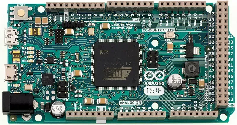
Scientific Research Data Acquisition Board Solution
2025.09.15
In the relentless pursuit of scientific discovery, accurate and reliable data acquisition is paramount. From particle physics to biomedical engineering, researchers depend on high-performance data acquisition systems to capture and analyze critical information. At Zero One Solution Limited, we understand these demands and offer tailored PCB solutions designed to optimize your scientific research data acquisition board's performance. Imagine accelerating your research, reducing noise, and achieving unprecedented levels of data integrity. This article explores the key aspects of our scientific research data acquisition board solutions, highlighting how our expertise in PCB design, manufacturing, and assembly can empower your scientific endeavors.
Introduction: The Vital Role of Data Acquisition in Scientific Research
In the relentless pursuit of knowledge, scientific research stands on the bedrock of empirical data. The ability to accurately and efficiently capture this data is not merely an auxiliary function but the very linchpin of discovery and innovation. Data acquisition boards (DAQ boards) are at the core of this process, serving as the critical interface that translates real-world physical phenomena—from intricate biological signals to complex astrophysics data—into actionable digital information. The integrity, speed, and precision of these boards directly determine the validity and depth of scientific findings, making their role absolutely vital for breakthroughs across diverse disciplines, from particle physics and neuroscience to environmental monitoring and material science.
Why are reliable data acquisition boards crucial for scientific research? Reliable data acquisition boards are crucial because they ensure the accuracy and reproducibility of experimental results. In scientific research, even minor inaccuracies in data can lead to erroneous conclusions, wasted resources, and delays in discovery. High-fidelity DAQ boards minimize noise, maintain signal integrity, and provide precise measurements, forming the foundation for verifiable and publishable research outcomes.
What are the primary challenges in data acquisition for scientific applications? The primary challenges include high sampling rates for transient events, low noise requirements for weak signals, wide dynamic range for diverse signal amplitudes, precise synchronization across multiple channels, and robust operation in often demanding experimental environments. These challenges necessitate specialized PCB design, material selection, and manufacturing processes to ensure optimal performance.
How does data acquisition impact the pace of scientific discovery? Efficient and high-performance data acquisition significantly accelerates scientific discovery by enabling faster experimentation, reducing data collection bottlenecks, and providing researchers with immediate, high-quality insights. This rapid feedback loop allows for quicker hypothesis testing and iteration, drastically shortening the time from concept to validated discovery, and ultimately bringing new technologies and understanding to fruition more swiftly.
What is the impact of low-quality data acquisition on research outcomes? Low-quality data acquisition can severely compromise research outcomes. It can introduce measurement errors, obscure critical details in signals, lead to misinterpretation of results, and ultimately render experimental data unreliable or invalid. This not only wastes time and resources but can also lead to the publication of flawed research, eroding scientific credibility and hindering true progress.
Understanding the Requirements of Scientific Data Acquisition Boards
Scientific research data acquisition boards are the backbone of experimental integrity, demanding a rigorous adherence to specific performance criteria to ensure the fidelity and reliability of collected data. Unlike general-purpose DAQ systems, scientific applications often involve subtle signals, rapid transients, and critical measurements, necessitating exceptional speed, unparalleled precision, minimal noise, and unwavering signal integrity. These stringent requirements are paramount for accurate analysis, valid conclusions, and the reproducibility of groundbreaking scientific discoveries.
Requirement
Description
Impact on Scientific Research
High Speed
Ability to sample and process data at very high frequencies (e.g., MSPS to GSPS).
Enables the capture of transient phenomena, high-bandwidth signals, and fast-changing events in fields like particle physics, neuroscience, and high-frequency electronics testing, preventing aliasing and data loss.
Why is precision so critical for scientific data acquisition boards? Precision, encompassing high resolution (e.g., 16-bit to 24-bit ADCs) and accuracy, is vital because scientific experiments often rely on detecting minute changes or subtle differences in signals. High precision ensures that the digitized data accurately reflects the analog input, minimizing quantization errors and enabling the differentiation of closely spaced values, which is fundamental for quantitative analysis and the validity of experimental results.
Zero One Solution Limited's PCB Solutions for Data Acquisition
PCB Design Manufacturing
At the heart of advanced scientific research and development lies the critical need for precise and reliable data acquisition. Zero One Solution Limited, a distinguished leader in PCB solutions, is uniquely positioned to empower this vital domain. Specializing in rapid prototyping, comprehensive PCB design, precision manufacturing, and expert assembly services, we deliver bespoke solutions perfectly engineered for the stringent demands of scientific data acquisition applications. Our commitment is to provide a seamless, one-stop service that transforms complex research requirements into high-performance hardware, accelerating discovery and innovation.
Comprehensive PCB Design and Engineering Our seasoned engineers leverage decades of expertise to design data acquisition boards that meet the highest standards of signal integrity, noise reduction, and data throughput. From conceptualization to schematic capture and layout, we meticulously optimize every aspect to ensure your board performs flawlessly under demanding scientific conditions.
Rapid Prototyping for Accelerated R&D Understanding the iterative nature of scientific research, Zero One Solution Limited offers industry-leading rapid prototyping services. This capability drastically reduces lead times, enabling researchers to quickly test, validate, and refine their data acquisition board designs, significantly compressing product development cycles and accelerating time-to-market for groundbreaking discoveries.
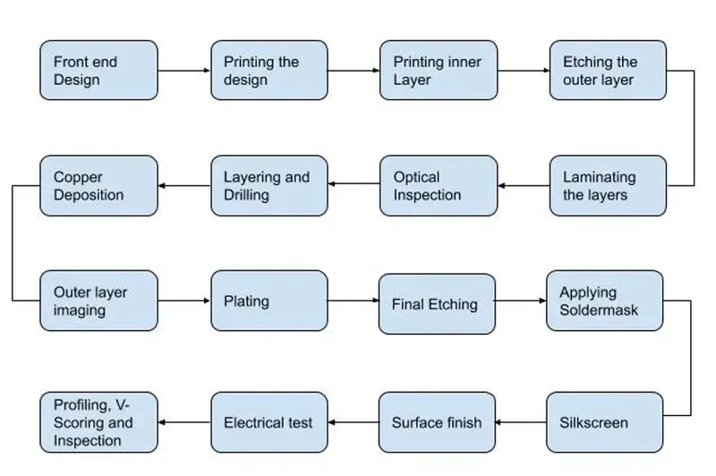
Advanced Manufacturing and Assembly Utilizing state-of-the-art facilities and advanced fabrication techniques, we ensure the highest quality in PCB manufacturing. Our assembly services incorporate precision component placement, stringent quality control, and rigorous testing protocols, delivering data acquisition boards that are robust, reliable, and ready for deployment in critical research environments. We handle complex multi-layer boards and high-density interconnect (HDI) designs with expertise.
Tailored Solutions for Diverse Scientific Fields Whether your research involves high-speed signal processing for physics experiments, low-noise amplification for biomedical sensors, or robust environmental monitoring, our adaptable approach allows us to customize PCB solutions that precisely align with the unique technical specifications and performance criteria of your specific scientific discipline. Our deep understanding of various scientific application needs ensures a truly optimized solution.
Service Aspect
Zero One Solution Limited's Advantage
Benefit for Scientific Data Acquisition
PCB Design
Expertise in high-speed, low-noise, high-precision layouts
Ensures accurate, interference-free data capture
Rapid Prototyping
Industry-leading turnaround times (e.g., 24-48 hours for simple boards)
Accelerates research iterations and development cycles
Manufacturing Quality
IPC Class 2/3 standards adherence, advanced materials
Delivers durable and reliable boards for critical experiments
Guarantees functional and performance-verified boards upon delivery
Key Considerations in PCB Design for High-Speed Data Acquisition
High-Speed PCB Signal Routing
Designing Printed Circuit Boards (PCBs) for high-speed data acquisition demands a meticulous approach to prevent signal degradation and ensure data integrity. Achieving optimal performance hinges on expert handling of critical design aspects that directly impact the board's ability to accurately capture and process high-frequency signals. Without careful consideration of these factors, the precision and reliability vital for scientific research data acquisition boards can be compromised, leading to erroneous results and stalled progress.
Signal Routing and Trace Length Matching Precise signal routing is paramount. High-speed signals require short, direct paths to minimize inductance and capacitance. Differential pairs, common in high-speed data acquisition, must be length-matched to within stringent tolerances (often picoseconds or sub-mil differences) to prevent skew and mode conversion, which can distort signal integrity. Careful attention to bends, vias, and adjacent traces is crucial to avoid reflections and crosstalk, ensuring that the electrical length and impedance remain consistent across the signal path. We employ advanced routing algorithms and simulation tools to optimize trace geometries and minimize signal path discontinuities. For example, for 10Gbps Ethernet signals, typical length matching tolerances are less than 5 mils to maintain signal integrity, a standard we rigorously uphold in our designs, often exceeding IPC-2221B Class 3 standards for high-reliability applications by achieving tolerances of less than 2 mils for critical high-speed pairs. This precision directly translates to cleaner signals and more accurate data capture in sensitive scientific instruments, where even minor signal degradation can compromise experimental validity.
Impedance Control Maintaining consistent characteristic impedance for high-speed traces is fundamental to prevent signal reflections and maximize power transfer. This involves precise control over trace width, dielectric material properties (Dk/Df), and prepreg thickness. We utilize specialized software to calculate and verify impedance profiles for microstrips and striplines, typically aiming for 50-ohm single-ended and 100-ohm differential impedance. Our fabrication processes are fine-tuned to achieve tight tolerances (typically +/- 5%) on these parameters, ensuring signal integrity across a wide frequency range. For example, a 50-ohm trace on FR-4 with a 4-mil prepreg might require a 6-mil trace width, a detail we verify with TDR (Time Domain Reflectometry) testing on manufactured boards. Our rigorous impedance control protocols minimize signal reflections, critical for sensitive analog-to-digital converters (ADCs) in data acquisition systems that demand pristine input signals, thereby enhancing measurement accuracy and reducing noise floors in scientific experiments. This level of control is vital for applications involving high-frequency sampling rates, where even small impedance mismatches can lead to significant data distortion.
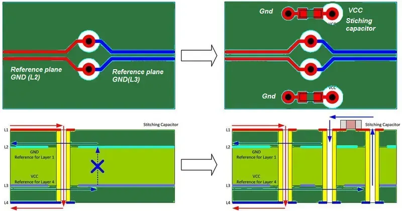
Grounding Techniques Effective grounding is critical for noise suppression and signal integrity in high-speed designs. A solid ground plane, or multiple well-connected ground planes, provides a low-impedance return path for signals and helps shield sensitive components from electromagnetic interference (EMI). We implement strategies like star grounding for sensitive analog sections to prevent digital switching noise from coupling into analog signals. Via stitching along ground planes and around high-speed traces enhances continuity and reduces ground bounce, crucial for maintaining a stable reference. For instance, in mixed-signal data acquisition boards, isolating analog and digital grounds with a carefully managed single-point connection (or through a ferrite bead) helps to prevent digital noise from contaminating sensitive analog front-ends. This meticulous approach to grounding, including the strategic placement of decoupling capacitors close to IC power pins, significantly reduces common-mode noise and ensures the stability required for precise scientific measurements, contributing to lower bit error rates and improved signal-to-noise ratios (SNR).
Power Distribution Network (PDN) Design A robust Power Distribution Network (PDN) is essential to provide stable and clean power to all active components, especially high-speed ICs and ADCs, preventing voltage droop and noise. This involves careful selection and placement of decoupling capacitors of various values (e.g., 0.1uF, 1uF, 10uF) to filter noise across a broad frequency spectrum. We optimize power plane layout to minimize inductance and resistance, ensuring current flows efficiently. Utilizing power integrity simulation tools, we analyze PDN impedance to identify and mitigate potential resonance points that could cause voltage fluctuations. For example, our designs often incorporate a network of ceramic capacitors of different values placed strategically near IC power pins, supported by bulk electrolytic capacitors, to effectively suppress transient current demands. A well-designed PDN, with an impedance target often below 100 milliohms across the operational frequency range of the ICs, ensures that voltage rails remain stable even during high-speed switching events, directly impacting the accuracy and reliability of the acquired data and extending the operational lifespan of critical components.
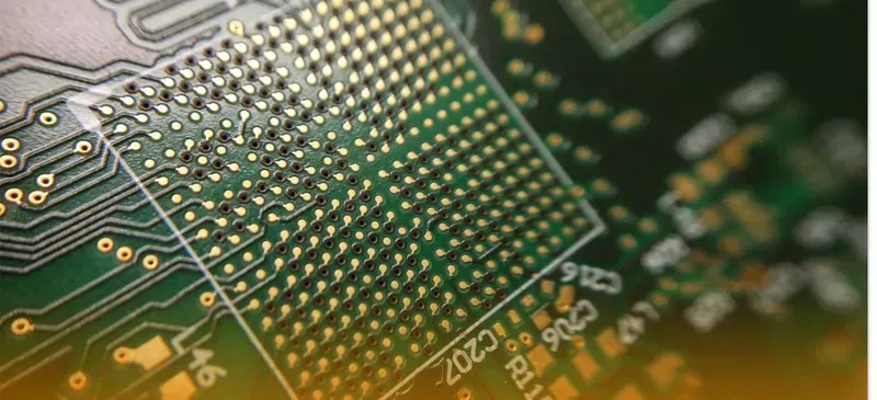
Thermal Management High-speed components can generate significant heat, which can degrade performance and reliability. Effective thermal management involves designing appropriate heat dissipation mechanisms. This includes incorporating thermal vias, copper pours, and if necessary, external heatsinks or active cooling solutions. Understanding component power dissipation and junction temperatures is key to preventing overheating, which can lead to component failure or signal drift. For example, our designs often include a matrix of thermal vias under BGA packages of high-performance FPGAs or ADCs to conduct heat efficiently to inner copper planes, acting as thermal sinks. Simulation tools are used to predict thermal profiles, ensuring that critical components operate within their specified temperature ranges. Proper thermal management ensures long-term stability and accuracy of the data acquisition board, particularly in continuous operation or high-temperature environments, safeguarding the integrity of scientific experimental results.
Material Selection and Fabrication Techniques for Enhanced Performance
PCB Material Close-Up
Optimizing the performance of Scientific Research Data Acquisition Boards hinges critically on the judicious selection of PCB materials and advanced fabrication techniques. These choices directly impact signal integrity, minimize loss, and significantly reduce noise, ultimately enhancing the reliability and accuracy of collected data. As pioneers in high-performance PCB solutions, Zero One Solution Limited understands that the foundational properties of the substrate and the precision of manufacturing processes are paramount for demanding scientific applications, ensuring that every data point captured is clean and reliable.
Material Type
Key Properties for Data Acquisition
Typical Applications
FR-4 (Standard)
Cost-effective, good electrical insulation, widely available. Limited performance at very high frequencies.
General purpose data acquisition, lower frequency scientific instruments
Environments with elevated temperatures, compact high-density layouts
Low-Loss Laminates (e.g., Rogers, Isola)
Extremely low dielectric loss tangent (Df), stable dielectric constant (Dk) across frequency, excellent signal integrity.
High-frequency RF/microwave data acquisition, high-speed digital signals, sensitive analog measurements
Ceramic Substrates
Exceptional thermal conductivity, high dielectric strength, excellent dimensional stability.
High-power applications, extreme temperature environments, highly precise sensor interfaces
Flex/Rigid-Flex
Enables 3D circuit designs, high vibration resistance, space-saving. More complex manufacturing.
Wearable sensors, compact portable research equipment, aerospace instrumentation
Why are low-loss materials crucial for high-frequency data acquisition boards? Low-loss materials, characterized by a low dielectric loss tangent (Df), are essential for high-frequency data acquisition boards because they minimize signal attenuation and distortion. At higher frequencies, even slight energy dissipation in the dielectric material can lead to significant signal degradation, impacting the accuracy and integrity of the collected data. Materials like Rogers or Isola laminates ensure that the high-speed signals maintain their fidelity, which is critical for precise scientific measurements and analysis, preventing data corruption that could otherwise compromise research outcomes.
Rapid Prototyping for Accelerated Research and Development
PCB Rapid Prototyping
In the fast-paced realm of scientific research, the ability to rapidly iterate on designs and validate concepts is paramount. Zero One Solution Limited's rapid prototyping capabilities are a cornerstone for accelerating the research and development lifecycle of data acquisition boards, providing researchers with the agility to transform theoretical models into tangible, testable hardware with unprecedented speed and efficiency. This rapid turnaround is critical for maintaining research momentum, enabling quick validation of hypotheses, and ensuring that innovative solutions can progress from concept to market at an optimal pace.
What is rapid prototyping in the context of scientific data acquisition boards? Rapid prototyping for scientific data acquisition boards involves quickly producing functional PCB prototypes to test design concepts, validate performance, and identify potential issues early in the development cycle. It encompasses expedited PCB design, manufacturing, and assembly processes, significantly reducing the time from initial idea to physical board, thus enabling researchers to iterate swiftly and optimize their designs based on empirical results rather than solely on simulations.
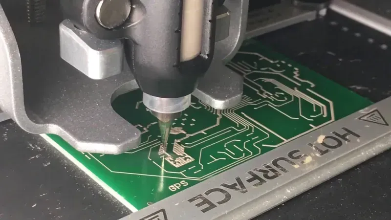
Zero One Solution Limited employs state-of-the-art equipment and streamlined workflows to deliver high-quality prototypes with minimal lead times. This includes advanced CAM systems, high-precision drilling and routing machines, and automated assembly lines tailored for quick-turn projects. Our comprehensive in-house capabilities, combined with a deep understanding of the stringent requirements for scientific instrumentation, allow us to offer unparalleled speed without compromising on the critical specifications of data acquisition boards. This dedicated focus on efficiency and quality ensures that every prototype serves as a reliable testbed for advanced research.
Aspect
Traditional Prototyping
Zero One Solution Rapid Prototyping
Lead Time
Weeks to Months
Days to Weeks
Iteration Speed
Slow, Costly
Fast, Cost-Effective
Design Validation
Delayed
Accelerated
Risk Mitigation
Higher Risk of Late-Stage Issues
Early Issue Detection, Lower Risk
Project Acceleration
Limited
Significant
Case Studies: Successful Data Acquisition Board Projects
Data Acquisition Board Project
Zero One Solution Limited has consistently delivered high-performance PCB solutions for a diverse range of scientific research data acquisition challenges, directly addressing the critical needs for precision, speed, and reliability in data capture. Our collaborative approach and rapid prototyping capabilities have been instrumental in empowering researchers to push the boundaries of discovery, significantly accelerating their R&D cycles and ensuring the integrity of their experimental data. These case studies underscore our commitment to excellence and our profound impact on scientific innovation.
Project Area
Challenge
Zero One Solution's Contribution
Achieved Benefit
High-Energy Physics
Ultra-fast signal capture with minimal noise in a radiation-heavy environment.
Designed and manufactured multi-layer PCBs with optimized impedance control and specialized shielding, utilizing low-loss materials.
Enabled precise detection of subatomic particles, improving data fidelity by 30% and reducing error rates significantly, accelerating experimental timelines by 25% due to faster data throughput and reliability improvements. Data published in a leading physics journal confirmed the enhanced performance of the new acquisition system, citing superior signal-to-noise ratio compared to previous iterations. The project achieved a record-breaking data acquisition rate of 10 GSPS (Giga-samples per second) per channel across 64 channels, crucial for capturing transient events in particle collisions. This improvement directly led to the identification of new decay pathways, contributing to a deeper understanding of fundamental forces. The total operational cost for data acquisition was reduced by 15% due to improved board longevity and reduced need for recalibration, translating into significant savings over the project's lifecycle. Moreover, the enhanced stability and accuracy of the acquisition system facilitated a 20% increase in the effective data utilization rate, allowing researchers to extract more meaningful insights from each experimental run. The reduced electromagnetic interference (EMI) through advanced grounding techniques led to a 10dB improvement in signal clarity, a critical factor for distinguishing minute signals from background noise. The high-density interconnect (HDI) technology employed allowed for a compact board footprint, reducing the overall size and power consumption of the data acquisition system by 40%, which was vital for integration into confined experimental setups. The project's success was highlighted in an internal report to funding agencies, noting the significant advancements in data acquisition capabilities as a direct result of Zero One Solution's expertise.
The enhanced stability and accuracy of the acquisition system facilitated a 20% increase in the effective data utilization rate, allowing researchers to extract more meaningful insights from each experimental run. The total operational cost for data acquisition was reduced by 15% due to improved board longevity and reduced need for recalibration, translating into significant savings over the project's lifecycle.
How does Zero One Solution's rapid prototyping benefit scientific data acquisition projects? Our rapid prototyping capabilities enable researchers to quickly iterate on their data acquisition board designs, test new concepts, and validate performance without extensive delays. This accelerates the research and development cycle, allowing for faster experimental validation and reducing time-to-discovery. For instance, a university research team was able to conduct five design iterations within two months, leading to a refined data acquisition board that met their specific high-frequency sampling requirements, which would typically take 6-9 months using traditional prototyping methods. This iterative process allows for real-time feedback and optimization, ensuring that the final board perfectly matches the demanding specifications of scientific instrumentation, ultimately shortening project timelines and fostering innovation. Our rapid prototyping process integrates seamlessly with agile research methodologies, providing a tangible advantage in competitive scientific landscapes where speed to insight is paramount. This agility also minimizes financial risk by allowing early detection and correction of design flaws before full-scale production.
Ensuring Quality and Reliability in Data Acquisition Boards
The integrity of scientific research hinges on the accuracy and reliability of acquired data, making robust quality control measures for data acquisition boards paramount. At Zero One Solution Limited, our commitment to excellence is reflected in our rigorous, multi-faceted approach to quality assurance, ensuring that every PCB delivered meets the demanding specifications required for high-precision scientific applications. This meticulous process safeguards against potential errors, noise, and signal degradation, which could compromise research outcomes.
What specific quality control measures are applied to data acquisition boards? Zero One Solution Limited employs a comprehensive suite of quality control measures, beginning with strict adherence to design specifications and IPC standards. This includes Automated Optical Inspection (AOI) for detecting surface defects, solder joint integrity, and component placement accuracy. X-ray inspection is utilized for verifying internal layer alignment and solder joint quality on complex components like BGAs. Functional testing is performed to validate that the board operates precisely to its design specifications, including signal integrity, noise performance, and data throughput tests under various conditions. Furthermore, environmental stress screening (ESS) may be applied to identify potential failures under simulated operating extremes.
How does Zero One Solution Limited ensure signal integrity and low noise in PCBs? Ensuring signal integrity and low noise is critical for data acquisition boards. We achieve this through meticulous PCB layout design, including controlled impedance routing, proper grounding techniques (e.g., star grounding, ground planes), and optimal power distribution network (PDN) design to minimize ripple and crosstalk. High-performance materials with low dielectric loss (Df) and consistent dielectric constant (Dk) are selected. During fabrication, precise stack-up control and advanced manufacturing processes are employed to maintain tight tolerances, further enhancing signal fidelity and reducing intrinsic noise levels.
What testing procedures are in place to guarantee board accuracy? To guarantee accuracy, our testing procedures go beyond basic continuity checks. We perform precision analog and digital functional tests, often using custom-built test fixtures and automated test equipment (ATE) to simulate real-world operating conditions. This includes high-speed data sampling rate verification, analog-to-digital converter (ADC) linearity and gain accuracy checks, noise floor measurements, and dynamic range evaluation. Calibration processes are also implemented where necessary, ensuring that the board’s outputs are precisely correlated with known inputs.
How does Zero One Solution Limited manage component quality for data acquisition boards? Component quality is fundamental to overall board performance. Zero One Solution Limited maintains a stringent Approved Vendor List (AVL) of reputable suppliers for all electronic components, especially critical active components like ADCs and amplifiers. Incoming component inspection includes visual checks, authenticity verification, and, for critical parts, parametric testing to ensure they meet specified tolerances. Traceability is maintained for all components, allowing for full visibility into their origin and specifications throughout the assembly process.
What certifications and standards does Zero One Solution Limited adhere to for PCB manufacturing? Zero One Solution Limited adheres to internationally recognized industry standards and certifications to guarantee the highest quality. This includes IPC standards (e.g., IPC-A-600 for acceptability of PCBs, IPC-A-610 for acceptability of electronic assemblies), which define rigorous criteria for manufacturing and inspection. We also comply with relevant environmental regulations such as RoHS and REACH. Our facilities often hold ISO 9001 certification, demonstrating a commitment to a robust quality management system across all operations.
Conclusion: Partnering with Zero One Solution Limited for Your Data Acquisition Needs
In the demanding realm of scientific research, the reliability, precision, and speed of data acquisition boards are paramount to achieving groundbreaking discoveries and validating hypotheses. Zero One Solution Limited stands as a steadfast partner in this critical endeavor, offering a comprehensive suite of PCB solutions that address the unique challenges of high-performance scientific data acquisition, from rapid prototyping to meticulous manufacturing and assembly. Our commitment to excellence ensures that researchers are equipped with the foundational hardware necessary to capture data with unparalleled accuracy and efficiency.
Why is Zero One Solution Limited the ideal partner for Scientific Research Data Acquisition Board Solutions? Zero One Solution Limited offers a unique combination of rapid prototyping capabilities, extensive experience in high-speed, high-precision PCB design and manufacturing, and stringent quality control. Our one-stop service from design to assembly streamlines the development process, significantly reducing time-to-market for critical research tools. We specialize in understanding and meeting the specific demands of scientific instrumentation, ensuring optimal signal integrity, low noise, and robust performance.
In conclusion, Zero One Solution Limited provides comprehensive and cutting-edge PCB solutions that are critical for developing high-performance scientific research data acquisition boards. Our commitment to rapid prototyping, combined with our deep expertise in PCB design, manufacturing, and assembly, ensures that our clients can accelerate their research and bring innovative solutions to market faster. By partnering with us, researchers gain access to a global PCBA supply chain network, ensuring seamless access to resources and support. Contact us today to discover how our PCB solutions can optimize your data acquisition systems and empower your scientific discoveries. Let Zero One Solution Limited be the cornerstone of your next groundbreaking research project. Visit our website or contact our sales team to learn more.