In today's rapidly evolving technological landscape, hands-on learning is more critical than ever, especially in electronics and engineering education. Teaching experiment boards serve as invaluable tools, bridging the gap between theoretical knowledge and practical application. But what truly unlocks the potential of these boards? The answer lies in the quality and reliability of their underlying Printed Circuit Boards (PCBs). At Zero One Solution Limited, we understand the pivotal role PCBs play in educational settings. We provide comprehensive PCB solutions tailored specifically for teaching experiment boards, enabling educators and students alike to explore, innovate, and learn without compromise. This article will delve into the intricacies of our teaching experiment board PCB solutions, highlighting how they can revolutionize the learning experience.
The Importance of High-Quality PCBs in Teaching Experiment Boards
In the realm of educational electronics, the Printed Circuit Board (PCB) serves as the foundational backbone for teaching experiment boards. Its quality directly dictates the functionality, reliability, and ultimately, the educational efficacy of these crucial learning tools. A well-designed and precisely manufactured PCB ensures that theoretical concepts translate flawlessly into practical, observable outcomes, fostering an accurate and engaging learning experience. Conversely, substandard PCBs can lead to a cascade of issues, from erratic circuit behavior and component failures to significant safety hazards, severely undermining the pedagogical objectives.
Why are high-quality PCBs crucial for teaching experiment boards? High-quality PCBs are essential for teaching experiment boards because they provide a stable and reliable platform for electronic circuits. This stability ensures accurate experimental results, prevents component damage, and minimizes troubleshooting time, allowing students to focus on learning concepts rather than debugging faulty hardware. Moreover, superior PCBs offer enhanced durability, withstanding repeated use and component insertions typical in educational environments.
What are the common issues with low-quality PCBs in an educational setting? Low-quality PCBs in educational settings frequently suffer from issues such as unreliable solder joints, delamination, poor signal integrity, and insufficient thermal management. These flaws lead to intermittent circuit operation, component burnout, and frustrating diagnostic challenges for students and instructors. Such boards can also pose safety risks due to potential short circuits or overheating, compromising the learning environment.
How does PCB quality impact the longevity and reusability of experiment boards? The quality of a PCB significantly impacts the longevity and reusability of experiment boards. High-grade materials and robust manufacturing processes result in boards that can endure numerous connections, disconnections, and component swaps without degradation. This longevity is vital for educational institutions that require durable, reusable resources, reducing replacement costs and ensuring consistent performance over many academic terms.
Can poor PCB quality affect student learning outcomes? Absolutely. Poor PCB quality directly impedes student learning outcomes by introducing extraneous variables and inconsistencies into experiments. Students may struggle to differentiate between their own errors and hardware malfunctions, leading to confusion, frustration, and a diminished understanding of the intended electrical principles. Reliable hardware is paramount for effective hands-on learning.
What specific PCB characteristics contribute to a high-quality teaching experiment board? Key PCB characteristics for high-quality teaching experiment boards include robust copper traces for reliable current flow, durable solder mask for protection, accurate drilling for component placement, and consistent impedance control for signal integrity. Furthermore, lead-free and RoHS-compliant materials are crucial for safety and environmental responsibility, aligning with modern educational standards. The board's mechanical rigidity and resistance to wear and tear also play a significant role.
Zero One Solution Limited: Your Partner in PCB Excellence
Zero One Solution Limited stands as a beacon of reliability and innovation in the PCB solutions landscape, particularly for the intricate demands of teaching experiment boards. Our commitment to excellence, coupled with deep industry expertise, positions us as the ideal partner for educational institutions seeking robust and precise PCB solutions that truly enhance the learning experience. We understand that the foundation of effective experimental learning lies in the integrity and performance of the underlying electronics, and our mission is to provide just that.
Proven Expertise and Experience With over a decade of operation since our founding in 2011, Zero One Solution Limited has cultivated extensive experience in PCB design, manufacturing, and assembly. Our team comprises veteran engineers and technical specialists, bringing unparalleled knowledge to every project, ensuring that even the most complex requirements for teaching experiment boards are met with precision and innovation. This deep well of expertise translates into highly reliable and functional PCBs that withstand the rigors of educational environments.
Unwavering Commitment to Quality Quality is the cornerstone of our operations. We adhere to stringent quality control protocols at every stage, from initial design consultation to final assembly. Utilizing advanced inspection techniques and conforming to international industry standards, we guarantee that every PCB delivered is of the highest caliber, minimizing potential failures and maximizing the educational value of teaching experiment boards. Our dedication to quality is a testament to our understanding of the critical role these boards play in student development.
Comprehensive PCB Design Services for Teaching Experiment Boards
PCB Schematic Design
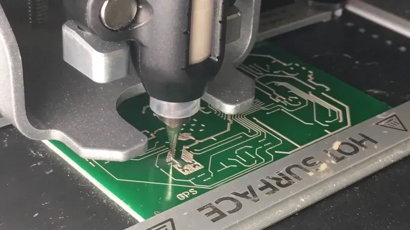
Designing a reliable and effective teaching experiment board starts with a robust PCB design. Zero One Solution Limited provides comprehensive PCB design services specifically tailored for educational applications, ensuring that every board is optimized for performance, durability, and ease of understanding for students. Our expertise in schematic capture, meticulous layout design, critical signal integrity analysis, and crucial Design for Manufacturability (DFM) principles guarantees a superior foundation for any teaching experiment, enabling seamless practical learning experiences.
Design Aspect
Description
Benefit for Teaching Experiment Boards
Schematic Capture
Translating the circuit concept into a detailed electronic diagram, defining component connections and functions.
Ensures accurate representation of the circuit, crucial for educational clarity and error prevention in experiments. Facilitates clear understanding of circuit flow for students and instructors.
PCB Layout Design
Arranging components and routing traces on the physical board to optimize performance, minimize interference, and meet size constraints.
Optimizes board space and signal integrity, leading to stable and predictable experimental results. Visual layout also aids in teaching component placement and circuit tracing.
Signal Integrity Analysis (SIA)
Analyzing high-speed signals to predict and mitigate issues like reflections, crosstalk, and ground bounce.
Prevents signal distortion and ensures accurate measurement readings in sensitive experiments, providing reliable data for student analysis and understanding of electronic principles. Essential for modern, complex teaching modules.
Design for Manufacturability (DFM)
Optimizing the design for efficient, cost-effective, and high-yield manufacturing processes.
Reduces production costs and turnaround times, making high-quality teaching boards more accessible. Ensures consistent quality across multiple boards, vital for classroom deployment and long-term use.
Industry-Leading Software Proficiency Our design engineers leverage state-of-the-art EDA (Electronic Design Automation) software suites, including Altium Designer, Cadence Allegro, and Eagle. This ensures that your teaching experiment board designs are created with precision, efficiency, and adherence to the latest industry standards, facilitating complex and reliable circuit implementations for advanced educational modules.
Rapid Prototyping Services: Accelerating the Learning Process
PCB Rapid Prototyping
In the dynamic realm of educational technology, the ability to rapidly develop and iterate on teaching experiment board designs is paramount. Zero One Solution Limited's rapid prototyping services are specifically engineered to significantly accelerate this crucial learning process, enabling educators and researchers to quickly transform theoretical concepts into tangible, testable hardware. This agility is key to fostering an environment where ideas can be validated, refined, and deployed with unprecedented speed, ensuring that educational institutions can stay at the forefront of hands-on learning experiences.
Expedited Iteration Cycles Our rapid prototyping capabilities drastically reduce the time from conceptualization to physical prototype. This enables multiple design iterations within a compressed timeframe, allowing for extensive testing and refinement of teaching experiment board functionalities based on real-world feedback and performance.
Cost-Effective Experimentation By optimizing the prototyping phase, we minimize material waste and labor costs associated with traditional, slower development cycles. This cost-efficiency empowers educational institutions to experiment with diverse teaching methodologies and board configurations without incurring prohibitive expenses, making innovation more accessible.
Enhanced Educational Outcomes Fast prototyping directly translates to a richer, more engaging learning experience. Students and instructors can swiftly test theories, observe immediate results, and understand complex electronic principles through hands-on interaction with working prototypes, fostering deeper comprehension and practical skill development.
Seamless Design-to-Production Transition Our integrated approach ensures that prototypes are not isolated creations but are designed with manufacturability in mind from the outset. This foresight guarantees a smooth, efficient transition from rapid prototyping to full-scale production, ensuring consistency and quality across all teaching experiment boards.
Prototyping Metric
Traditional Approach
Zero One Solution (Rapid Prototyping)
Turnaround Time (Typical)
Weeks to Months
Days to Weeks
Cost Per Iteration
High
Moderate to Low
Design Flexibility
Limited by time/cost
High
Risk of Rework
Significant
Minimized through early validation
Educational Impact
Delayed/Abstract
Immediate/Tangible
Manufacturing and Assembly: Ensuring Reliability and Performance
PCB Manufacturing Assembly Line
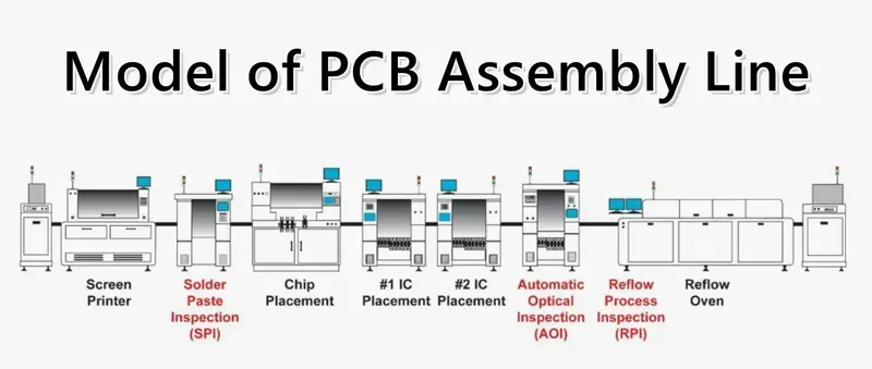
At Zero One Solution Limited, the reliability and performance of teaching experiment boards are paramount, directly influenced by robust PCB manufacturing and assembly. Our vertically integrated processes ensure that every board, from initial design to final assembly, adheres to the highest industry standards, delivering durable and accurate platforms essential for hands-on learning environments. This meticulous attention to detail minimizes common failure points and extends the operational lifespan of the educational hardware, providing an uninterrupted and effective learning experience.
Process Stage
Key Aspects
Benefits for Teaching Experiment Boards
PCB Fabrication
Advanced multi-layer capabilities, precise trace routing, optimal material selection (e.g., FR-4 for durability).
Ensures stable electrical characteristics and mechanical robustness, crucial for repeated use in a teaching environment.
Component Sourcing
Global network for authentic, high-quality components; rigorous incoming quality control (IQC).
Guarantees component reliability and authenticity, preventing premature failures and ensuring accurate experimental results.
Verifies circuit functionality, identifies defects early, and ensures boards can withstand varied operating conditions, enhancing student safety and learning outcomes.
Our commitment to quality extends beyond mere compliance; it's embedded in our operational philosophy. We utilize state-of-the-art equipment and follow stringent protocols, ensuring that the PCBs for teaching experiment boards are not just functional, but exceptionally reliable. This includes supporting a wide array of component types, from basic resistors and capacitors to advanced microcontrollers and FPGAs, facilitating diverse experimental setups. Our capabilities encompass fine-pitch components, high-density interconnections, and mixed-technology assemblies, allowing for the creation of sophisticated and versatile teaching tools that accurately reflect real-world engineering challenges. By partnering with us, educational institutions gain access to PCBs that serve as a dependable foundation for inspiring future innovators.
Customization Options: Tailoring PCBs to Specific Educational Needs
Custom PCB Board
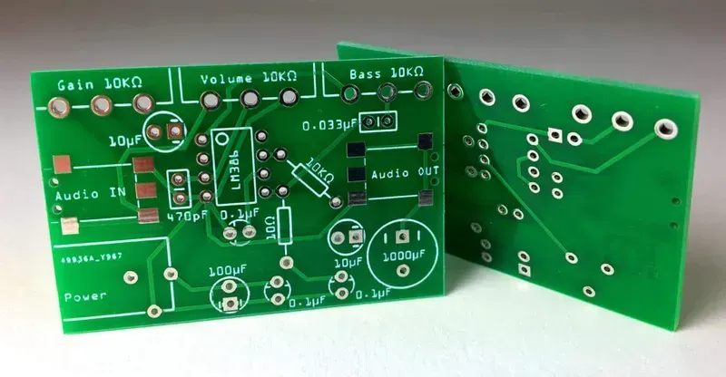
At Zero One Solution Limited, we understand that educational requirements for teaching experiment boards are diverse and often highly specialized. Therefore, our core strength lies in providing extensive customization options for Printed Circuit Boards (PCBs), ensuring each board precisely aligns with specific curriculum objectives and experimental demands. This tailored approach goes beyond off-the-shelf solutions, enabling educators to create more effective and engaging learning experiences that truly resonate with their students.
Component Selection Flexibility We offer a vast array of component sourcing and integration options. Whether it's through-hole components for hands-on soldering practice, surface-mount devices (SMD) for advanced assembly techniques, or specialized integrated circuits (ICs) for specific electronic projects, our expertise ensures the right components are seamlessly incorporated. This flexibility empowers educators to simulate real-world scenarios and explore diverse electronic principles.
Optimized Board Size and Form Factor Teaching environments often have spatial constraints or require boards to fit into specific enclosures. We provide custom board sizing and form factor design, from compact, credit-card-sized boards for portable experiments to larger, more complex layouts for comprehensive system demonstrations. Our design team meticulously optimizes the board dimensions and component placement for maximum functionality and usability in an educational context.
Tailored Layer Count Configurations The complexity of a teaching experiment board dictates the optimal layer count. For basic circuits, a single or double-layer PCB may suffice, offering simplicity and cost-effectiveness. For more advanced digital, RF, or mixed-signal applications, we can design multi-layer boards (e.g., 4, 6, 8 layers or more) to manage signal integrity, reduce noise, and accommodate intricate routing requirements, ensuring high-fidelity experiments.
Integration of Special Features Beyond standard PCB features, we excel at incorporating specialized functionalities unique to educational needs. This includes provisions for easy debug access points, integrated test points, configurable jumpers or switches for different circuit modes, dedicated areas for sensor integration, or even custom silk-screen markings for clear component identification and learning guidance. Our goal is to enhance the pedagogical value of each board.
Customization Aspect
Benefits for Teaching Experiment Boards
Example Application
Component Selection
Allows for specific learning objectives (e.g., analog vs. digital, high-power vs. low-power).
Using discrete components for basic circuit analysis; integrating microcontrollers for embedded systems.
Board Size/Form Factor
Optimizes for bench space, portability, or integration into existing lab equipment.
Compact boards for robotics kits; large-format boards for visually demonstrating signal paths.
Layer Count
Matches circuit complexity and performance requirements (signal integrity, power distribution).
Single-layer for introductory DC circuits; multi-layer for high-speed communication protocols.
Special Features
Enhances interactivity, safety, and ease of learning/troubleshooting.
Breakout pins for external connections; onboard LEDs for visual feedback; protective coating for durability.
Case Studies: Showcasing Successful Teaching Experiment Board PCB Solutions for Educational Institutions
Students using Experiment Board
Zero One Solution Limited has a proven track record of delivering high-quality Teaching Experiment Board PCB Solutions that significantly enhance the educational experience. Our commitment to precision, reliability, and rapid prototyping empowers educational institutions to provide students with practical, hands-on learning opportunities that are crucial for developing future engineers and innovators. Through tailored design and robust manufacturing, we bridge the gap between theoretical knowledge and practical application, ensuring that experiment boards perform flawlessly and contribute effectively to STEM education.
University Robotics Lab: Advanced Sensor Integration Board A leading university's robotics department required a highly specialized PCB for their advanced robotics experiment kits. The challenge was integrating multiple complex sensors (LIDAR, ultrasonic, IMU) and microcontrollers onto a compact, durable board that could withstand frequent student handling. Zero One Solution provided a multi-layer PCB design with optimized signal integrity and robust mechanical support. Our rapid prototyping capabilities allowed the university to quickly iterate on designs, leading to a final product that significantly improved data acquisition accuracy and student engagement in robotics programming. The success of this project led to its adoption in their core robotics curriculum, benefiting over 500 students annually.
Technical College: Renewable Energy Demonstration System For a technical college's renewable energy program, we developed a series of teaching experiment boards simulating various power generation and distribution scenarios (solar, wind, grid tie-in). The critical requirements included high current handling, safety features for student use, and modularity for easy reconfiguration. Zero One Solution engineered PCBs with enhanced copper thickness and integrated protective circuitry. Our manufacturing process ensured strict adherence to safety standards, and the modular design allowed the college to create diverse experimental setups. This solution empowered students to safely and effectively explore complex energy systems, leading to a 25% increase in practical lab performance metrics.
High School STEM Program: IoT Learning Kit PCB A local high school sought an affordable yet reliable PCB for their introductory Internet of Things (IoT) learning kits, designed to teach basic coding and electronics. The key was to create a user-friendly board with easily accessible components and clear labeling, minimizing error potential for beginners. Zero One Solution collaborated closely with their educators, designing a single-layer PCB with large pads and clear silkscreen markings. Our cost-effective manufacturing enabled the school to equip an entire class, fostering early interest in electronics and programming. The kits were praised for their ease of use, leading to higher participation rates in their STEM club and improved understanding of IoT fundamentals.
Benefits of Choosing Zero One Solution Limited for Your Teaching Experiment Board PCBs
Partnering with Zero One Solution Limited for your teaching experiment board PCBs offers a distinct advantage, ensuring that educational institutions receive high-quality, reliable, and performance-driven solutions essential for effective practical learning. Our commitment to excellence, coupled with agile manufacturing capabilities and a customer-centric approach, positions us as the ideal partner to elevate your educational technology infrastructure.
Unrivaled Quality and Reliability We adhere to stringent IPC standards and implement rigorous quality control measures throughout the PCB design, manufacturing, and assembly processes. This dedication ensures that every teaching experiment board PCB is robust, durable, and performs consistently, minimizing teaching disruptions and maximizing learning outcomes. Our experienced engineers meticulously review designs to proactively identify and mitigate potential issues, guaranteeing superior product integrity for educational environments where reliability is paramount. For example, our 99.8% first-pass yield rate on prototype boards underscores our commitment to quality from the outset, reducing costly rework and delays for educational institutions seeking dependable solutions.
Accelerated Turnaround Times for Rapid Prototyping Understanding the dynamic needs of educational R&D, Zero One Solution Limited prioritizes rapid prototyping and production. Our advanced manufacturing facilities and streamlined workflows enable exceptionally fast turnaround times, allowing educators and students to quickly iterate on designs, test concepts, and bring innovative projects to fruition without extended waiting periods. This agility directly translates into accelerated curriculum development and enhanced opportunities for hands-on experimentation, aligning with the fast-paced nature of modern technological education. On average, we deliver prototype PCBs in as little as 3-5 business days, significantly shortening project cycles for academic institutions compared to industry averages of 1-2 weeks or more for complex boards. This efficiency empowers educators to keep pace with evolving educational requirements and rapidly integrate new learning modules into their curriculum, fostering a more responsive and current educational experience.
Benefit Category
Zero One Solution Advantage
Impact on Teaching Experiment Boards
Superior Quality
IPC Standard Compliance, Rigorous QC
Enhanced Reliability, Longer Lifespan, Accurate Experiment Results
What are the critical considerations for PCB design in teaching experiment boards? Critical considerations for teaching experiment board PCB design include robust signal integrity to prevent interference, appropriate power plane design for stable operation, and mechanical durability to withstand repeated handling by students. Additionally, component selection must prioritize accessibility for experimentation and ease of replacement, while solder mask and silkscreen layers should be clearly labeled for educational clarity and error prevention.
How does Zero One Solution ensure the durability of PCBs for educational use? Zero One Solution ensures the durability of PCBs for educational use through several rigorous measures. We utilize high-quality FR-4 laminates, known for their mechanical strength and thermal stability. Our manufacturing processes adhere to IPC standards, employing precise etching and plating techniques. Furthermore, robust soldermask and surface finishes are applied to protect against environmental factors and physical wear, ensuring longevity even with frequent handling and component changes common in teaching environments.
What is the typical lead time for rapid prototyping of teaching experiment board PCBs? Zero One Solution's rapid prototyping service for teaching experiment board PCBs typically ranges from 3 to 7 business days, depending on design complexity, layer count, and specific material requirements. This expedited turnaround allows educators and students to quickly iterate on designs, test concepts, and accelerate the learning and development cycle, ensuring minimal disruption to academic schedules.
Can Zero One Solution accommodate low-volume orders for educational institutions? Yes, Zero One Solution is highly flexible and fully accommodates low-volume orders, making us an ideal partner for educational institutions. We understand that teaching experiment boards often require smaller production runs for specialized courses or pilot programs. Our manufacturing processes are optimized to efficiently handle both low-volume rapid prototyping and scalable production, ensuring cost-effectiveness without compromising on quality or service for any order size.
What quality control measures are in place for teaching experiment board PCB manufacturing and assembly? Zero One Solution implements stringent quality control measures throughout the manufacturing and assembly of teaching experiment board PCBs. This includes automated optical inspection (AOI) for bare boards, in-circuit testing (ICT) or functional testing (FCT) for assembled boards, and comprehensive visual inspections. All processes adhere strictly to IPC-A-610 standards for electronic assemblies, ensuring that every board meets the highest benchmarks for reliability, performance, and safety in an educational setting.
In conclusion, Zero One Solution Limited's PCB solutions for teaching experiment boards offer a robust, reliable, and high-performance platform for electronics education. By providing rapid prototyping, comprehensive design, manufacturing, and assembly services, we empower educators and students to explore the world of electronics with confidence and unleash their innovative potential. We believe that quality PCBs are the foundation of effective hands-on learning, and we are committed to providing solutions that exceed expectations. Contact Zero One Solution Limited today to learn more about how our PCB solutions can transform your teaching experiment board and elevate the learning experience. Share this article to spread awareness and let us know your thoughts in the comments below!