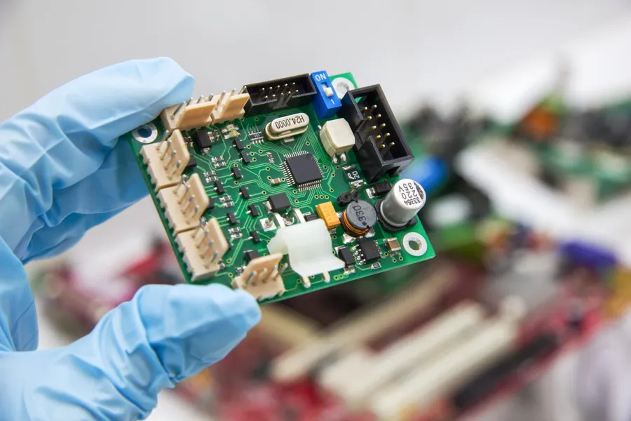
In today's technology-driven world, circuitry design is the invisible force behind every electronic device we use. From the simplest home appliances to sophisticated spacecraft, the art and science of designing circuits is fundamental. This article delves into the core concepts of circuitry design, exploring the process, best practices, and the tools used by professionals to create functional and innovative electronic systems. We'll explore not only the technical aspects but also the creative thinking behind transforming abstract ideas into tangible, working circuits. Let's open the door to understanding the elegant world of circuitry design that powers our modern world.
Understanding the Fundamentals of Circuitry Design
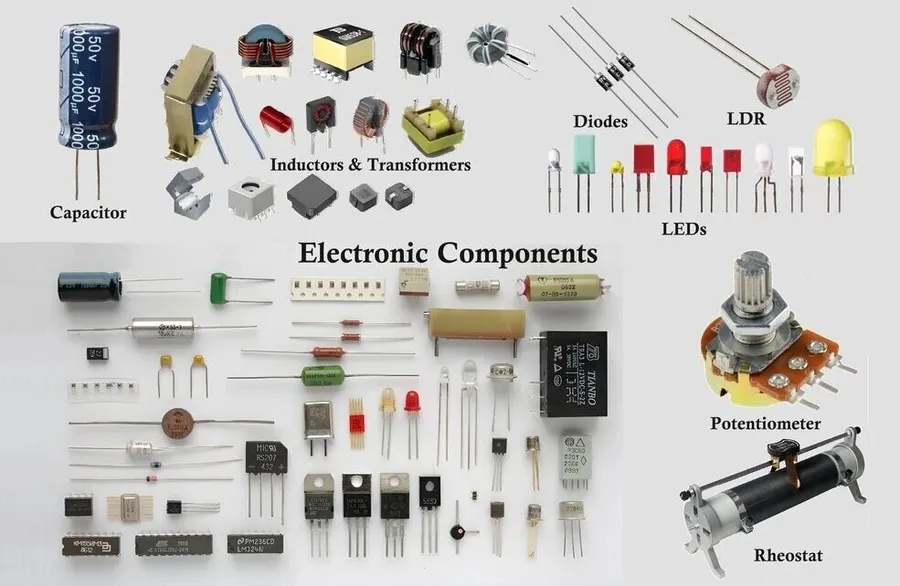
Electronic Components
Circuitry design, at its core, is the systematic process of creating electronic circuits to perform specific functions. This involves applying fundamental principles of physics and electronics, selecting appropriate components, and arranging them in a way that meets desired performance criteria. It's the bedrock of modern electronics, enabling everything from simple household gadgets to complex aerospace systems.
Key concepts in circuitry design include:
Ohm's Law Defines the relationship between voltage, current, and resistance in a circuit (V = IR).
Kirchhoff's Laws Kirchhoff's Current Law (KCL) states that the total current entering a junction must equal the total current leaving the junction; Kirchhoff's Voltage Law (KVL) states that the sum of voltages around a closed loop must equal zero. These laws are fundamental for circuit analysis.
Circuit Analysis Techniques Methods such as nodal analysis, mesh analysis, and superposition, used to solve for unknown voltages and currents in circuits.
Key Components Familiarity with components such as resistors (limit current), capacitors (store energy), inductors (oppose changes in current), diodes (allow current flow in one direction), and transistors (act as switches and amplifiers) is essential.
These fundamental concepts are not just theoretical exercises; they are practical tools used in the real world by engineers to design, analyse, and optimise circuit performance. A strong understanding ensures reliable, efficient, and effective electronic designs.
The Step-by-Step Circuitry Design Process
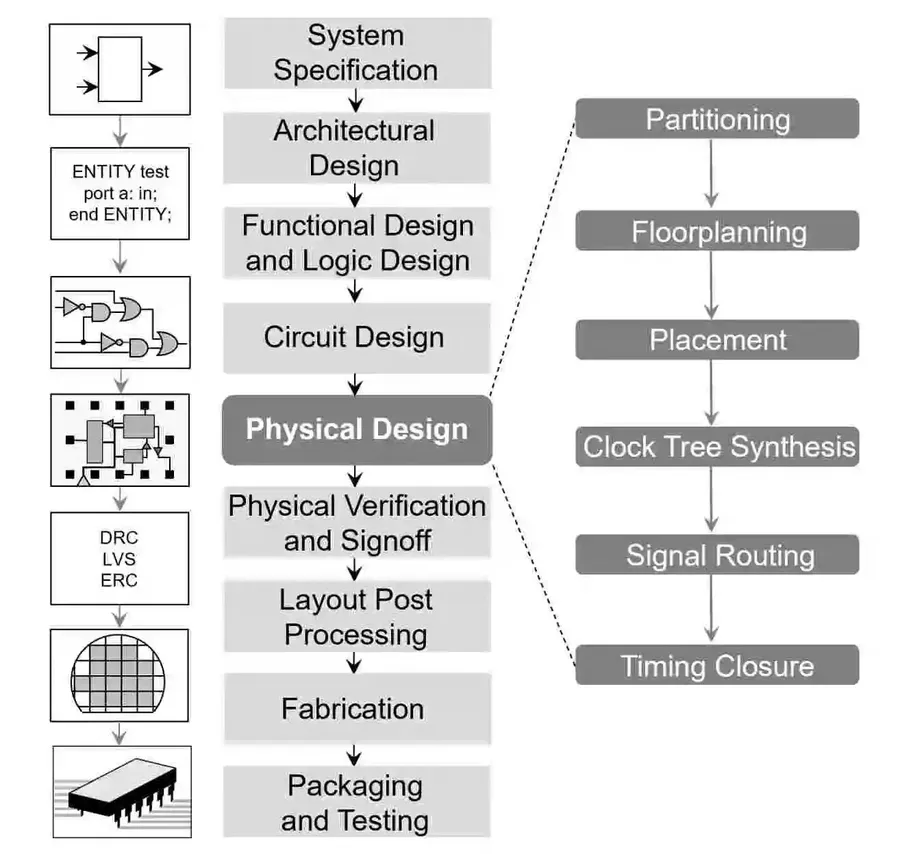
Circuit Design Flowchart
The creation of a functional circuit is an intricate, iterative process that demands a structured approach. It begins with a conceptualization of the circuit's purpose and culminates in a rigorously tested and validated physical realization. Each phase is crucial, and careful adherence to this process is essential for successful circuitry design.
1. Defining Specifications and Requirements The initial step involves a comprehensive understanding of the desired circuit's functionality, performance benchmarks, and application setting. This includes power requirements, input/output specifications, environmental constraints, and any applicable industry standards. Clear specifications at this stage are paramount to a successful design.
2. Conceptualization and Block Diagram Creation Here, the circuit's functionality is broken down into interconnected blocks, each representing a distinct function. These blocks are linked together in a block diagram to visualize the high-level architecture of the circuit, guiding the subsequent component selection and schematic capture.
3. Component Selection Based on the specifications and block diagram, appropriate electronic components like resistors, capacitors, transistors, and integrated circuits are chosen. This selection process considers factors like component ratings, tolerances, availability, and cost, ensuring each part aligns with performance and reliability needs.
4. Schematic Capture Using Electronic Design Automation (EDA) tools, a schematic diagram is created to detail the electrical connections between chosen components. This involves symbol selection, net listing, and ensuring all connections are accurate and logically organized.
5. Circuit Simulation Before physical implementation, the circuit's behavior is analyzed using simulation software. Tools such as SPICE are employed to verify functionality, check performance against specifications, and identify potential issues or areas for optimization. This step helps to mitigate costly errors during prototyping.
6. PCB Layout Design Once simulations are satisfactory, the schematic is used to design the physical Printed Circuit Board (PCB). This includes component placement, trace routing, and consideration of thermal and signal integrity issues. PCB design tools help ensure manufacturability and performance.
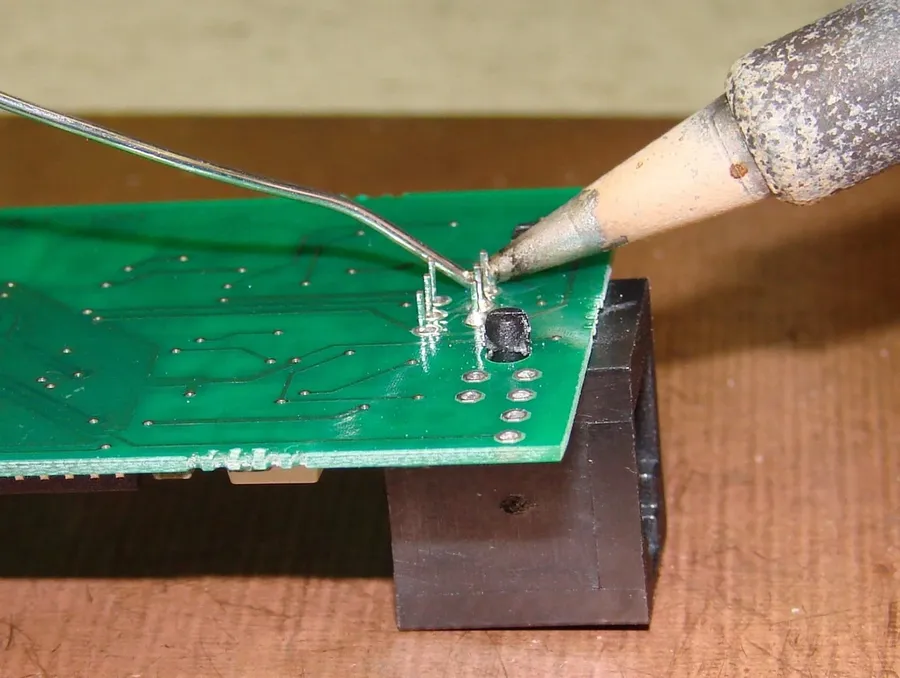
7. Prototyping The PCB design is then translated into a physical prototype, either through in-house assembly or external manufacturing. Components are soldered onto the fabricated board, marking a transition from virtual design to physical realization.
8. Testing and Validation The constructed prototype undergoes thorough testing, employing instruments like multimeters and oscilloscopes, to ascertain it performs as per defined specifications. This phase includes functional testing, performance evaluation, and environmental stress testing to ensure reliability. This data-driven approach provides crucial insights for any design revisions.
9. Design Iteration and Refinement Based on the test results, the design may be iterated by revisiting previous phases in the design process to further optimize the circuit performance. This iterative process might involve adjusting component values, improving PCB layout, or even revising the initial specifications.
Essential Tools and Software for Circuit Design
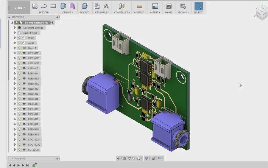
Circuit Design Software
Effective circuitry design relies heavily on specialized software tools that streamline the process from conceptualization to validation. These tools, encompassing Computer-Aided Design (CAD), Electronic Design Automation (EDA), and simulation platforms, enhance precision, reduce errors, and accelerate the design cycle.
Tool Category
Description
Examples
Typical Use Cases
CAD Software
Used for schematic capture and PCB layout, providing a visual interface for circuit design.
Choosing the right software depends on project complexity, budget, and familiarity with the tool. Free options like KiCad are excellent for smaller projects or hobbyists, while professional suites like Altium Designer or Cadence Allegro offer robust features for large-scale commercial designs. Furthermore, consider software which integrates multiple functions into one platform, such as Autodesk Fusion 360, which offers both CAD and CAM capabilities.
Best Practices in Electronic Circuit Design
Soldering PCB
Effective electronic circuit design hinges on adherence to best practices that ensure functionality, reliability, and longevity. These practices address common pitfalls and optimize performance by managing signal integrity, thermal considerations, power distribution, and component interactions, ultimately leading to robust and efficient electronic systems.
Proper Grounding Techniques Establishing a low-impedance ground plane is paramount. A solid ground reference reduces noise, prevents ground loops, and ensures stable operation. Use star grounding or a multi-layer PCB with dedicated ground layers to minimize impedance.
Decoupling Capacitors Place decoupling capacitors close to the power pins of integrated circuits to provide a local charge reservoir. These capacitors reduce voltage fluctuations and supply clean power to the IC, mitigating power rail noise and ensuring stable operation of sensitive components.
Thermal Management Heat dissipation is crucial for reliable operation and must be addressed by proper heatsinking and thermal vias. Calculate thermal budgets carefully and incorporate heat sinks for components with significant power dissipation. Use thermal vias to transfer heat from surface mounted components through the PCB to layers that have a higher capability to dissipate heat.
Signal Integrity Maintain signal integrity by minimizing trace lengths, using impedance-controlled traces for high-speed signals, and avoiding sharp bends. This reduces signal reflections, crosstalk and ensures clean signal transmission, which is particularly important in high-frequency circuits.
Component Selection Choose components that meet the design specifications and have appropriate ratings for voltage, current, and power dissipation. Always consider tolerances and ensure they are within the design margins to avoid any component damage or unpredictable behaviour
Best Practice
Description
Importance
Grounding
Low impedance ground plane
Reduces noise, prevents ground loops
Decoupling
Local charge reservoirs
Minimizes power rail noise and supply fluctuations
Thermal Management
Heat sinks and thermal vias
Dissipates heat, prevents overheating and component damage
Signal Integrity
Controlled trace impedance
Reduces signal reflections and crosstalk
Component Selection
Appropriate ratings and tolerances
Ensures reliability and avoids component failures
Optimizing Your Circuitry Design for Performance
Electronic Test Equipment
Optimizing circuitry design for performance is crucial for achieving efficient, reliable, and high-performing electronic systems. This involves a multifaceted approach, addressing power consumption, signal integrity, noise management, and overall operational efficiency through strategic design choices and techniques.
Several key areas require careful consideration to maximize circuit performance:
Power Consumption Reducing power consumption is essential for energy efficiency and thermal management. Techniques include utilizing low-power components, implementing power gating, and optimizing voltage levels.
Signal Noise Management Managing signal noise ensures signal integrity and reliable operation. Effective strategies include employing proper shielding, filtering, and differential signaling techniques to mitigate the effects of unwanted electrical noise.
Efficiency Enhancement Enhancing efficiency involves careful component selection and design layout to minimize losses. Strategies such as optimizing impedance matching, minimizing trace lengths, and careful component placement can significantly improve the efficiency of the circuit.
Impedance Matching Impedance matching is vital for maximizing power transfer and minimizing signal reflections in high-frequency circuits. Proper impedance matching minimizes signal loss and optimizes the performance of the system by ensuring that the source and load impedances are equal.
Shielding Shielding is a technique used to protect sensitive circuits from electromagnetic interference (EMI). By enclosing circuits in conductive materials, shielding limits the effects of external electromagnetic fields, thereby minimizing noise and improving reliability.
Optimization Area
Techniques
Impact
Power Consumption
Low-power components, power gating, voltage optimization
Reduced energy usage, lower heat generation, longer battery life
Signal Noise
Shielding, filtering, differential signaling
Improved signal integrity, more reliable operation, reduced errors
Printed Circuit Board (PCB) design is the cornerstone of modern electronics, transforming schematic diagrams into physical reality. This section provides a foundational understanding of PCB design, covering essential aspects from single-layer to multi-layer boards, trace routing, and component placement.
A well-designed PCB is crucial for the proper functioning and reliability of any electronic device. Poor PCB design can lead to signal integrity issues, thermal problems, and even complete circuit failure. Therefore, understanding the fundamentals of PCB design is paramount for any electronics engineer.
Feature
Single-Layer PCB
Multi-Layer PCB
Number of Layers
One conductive layer
Two or more conductive layers
Complexity
Simpler designs
Complex designs
Routing
Limited routing options
More routing options
Size and Density
Larger board size for same complexity
Higher component density and smaller form factor possible
Trace Routing Trace routing involves planning the path of conductive traces (copper tracks) on the PCB. Proper routing is essential for minimizing signal interference and impedance mismatches. Key aspects include trace width calculation, spacing and minimizing the length of high-speed signal traces.
Via Placement Vias are conductive pathways that allow electrical signals to travel between different layers of a multi-layer PCB. Strategic placement of vias is critical for efficient signal routing and thermal management. Considerations include via type (through-hole, blind, buried) and their impact on signal integrity and manufacturing cost.
Component Footprint Management Component footprints are the physical shapes and dimensions on the PCB where electronic components are mounted. Accurate footprint management ensures proper soldering and electrical connections. Component footprints adhere to standardized IPC specifications, ensuring interoperability and manufacturability. Proper component selection should include consideration for temperature and environmental factors in the PCB design.
Common Design Rules Design rules are a set of manufacturing constraints to ensure that the designed PCB is manufacturable and functional. These rules often depend on the manufacturing capabilities of the PCB fabrication facility. These rules define minimum trace widths, spacing, via diameters, and other parameters that must be adhered to for proper fabrication.
Troubleshooting and Debugging Circuitry Designs
Effective troubleshooting and debugging are critical for ensuring the reliability and functionality of circuitry designs. This section outlines systematic approaches to identify, analyze, and resolve common issues, utilizing essential tools and techniques for efficient diagnosis.
Debugging a circuit involves a structured approach that combines logical deduction with practical testing. It's crucial to first observe the symptoms carefully, then develop a hypothesis, test, and if needed iterate the process until the root cause is found.
Common Circuitry Issues: Identifying typical problems is crucial. These include signal integrity problems, such as reflections and crosstalk, power distribution issues causing voltage drops and noise, and component failures stemming from manufacturing defects or exceeding operational limits.
Essential Testing Tools: Tools like multimeters are fundamental for measuring voltage, current, and resistance. Oscilloscopes are used to visualize signal waveforms, assess signal quality, and detect timing issues. Logic analyzers help examine digital signals and protocol behavior.
Debugging Techniques: Start by visually inspecting the circuit for obvious issues such as solder bridges or incorrectly placed components. Then check the power supply for the correct voltage levels, use signal tracing to follow the signal path and determine where problems originate. Employ divide and conquer method by dividing the circuit into smaller functional blocks and troubleshooting each block in isolation.
Issue
Possible Causes
Troubleshooting Steps
No Power
Power supply failure, blown fuse, short circuit
Verify power supply output, check fuses, isolate short circuits
Signal Distortion
Improper impedance matching, reflections, noise
Check signal integrity, verify impedance matching, add filtering
This section addresses common queries regarding circuitry design, providing concise answers to help clarify fundamental concepts and practical aspects of the field. These questions are crucial for both beginners and experienced practitioners looking to solidify their understanding.
What exactly is circuitry design? Circuitry design involves planning and creating the pathways for electrical current to flow within a device or system, utilizing components like resistors, capacitors, and transistors to perform specific functions. It's about strategically arranging these elements to achieve a desired electrical behavior or outcome, whether it's powering a simple light or a complex computer.
How difficult is it to learn circuitry design? The difficulty in learning circuitry design depends on an individual's background and the depth of understanding they wish to achieve. Basic circuit design principles can be grasped with a fundamental understanding of physics and mathematics. However, advanced design involving complex systems and signal integrity requires years of experience and in-depth technical knowledge. Consistent practice and learning from real-world examples are crucial for mastering the art of circuitry design.
What steps should I take to become a circuit designer? A career in circuit design typically involves formal education in electrical engineering or a related discipline, followed by practical experience. Begin by mastering fundamental electrical concepts, understanding circuit analysis, and familiarizing yourself with simulation tools. Pursuing internships or entry-level positions can further enhance one's practical skills and understanding, followed by more advanced certifications or postgraduate degrees for specialist roles.
What are the key factors to consider for a successful circuitry design? A robust circuitry design takes into account several key factors: the intended function of the circuit, the performance requirements (speed, power consumption, noise), environmental conditions (temperature, humidity), and cost constraints. Component selection is crucial, as is ensuring compatibility, and thermal management must also be considered for reliable operation. Furthermore, manufacturability and testability are important considerations for production and maintenance.
Which software tools are most important for circuit design? Essential software tools for circuit design include Electronic Design Automation (EDA) software for schematic capture and simulation, Computer-Aided Design (CAD) software for PCB layout, and specialized simulation tools for analyzing signal behavior. Proficiency in these tools enables accurate and efficient design and testing, streamlining the development process, such as Autodesk Fusion, or Altium Designer.
What is the role of simulation in circuitry design? Simulation is critical in circuitry design as it allows engineers to test and refine their designs before they are physically built. Simulation software helps identify potential flaws, optimize performance, and reduce costs and development time by simulating real-world conditions and predicting circuit behavior under different operating parameters and scenarios.
How does PCB design relate to overall circuitry design? Printed Circuit Board (PCB) design is an essential part of the overall circuitry design process because it is the physical medium that supports and connects electrical components to form a functional electronic circuit. Efficient PCB design ensures optimal circuit performance, proper routing, signal integrity, and reliable operation. Considerations during PCB design include layout, layer stackup, thermal management, and manufacturability.
The Future of Circuitry Design
The field of circuitry design is rapidly evolving, driven by advancements in technology and increasing demands for more efficient, compact, and intelligent electronic systems. The future promises significant shifts in how circuits are designed, fabricated, and used across various industries.
Key trends shaping the future of circuitry design include:
AI-Driven Design Tools Artificial intelligence (AI) and machine learning (ML) are increasingly being integrated into design software. These tools can automate complex tasks such as component placement, routing, and optimization, significantly reducing design time and improving circuit performance. AI algorithms can also predict potential design flaws and suggest solutions, enhancing design reliability.
Miniaturization and Nanotechnology The demand for smaller, more portable electronic devices is driving the push for miniaturization. Nanotechnology is playing a crucial role in creating increasingly smaller and more efficient electronic components and circuits, enabling the development of highly compact devices and systems. This includes advances in materials science and fabrication techniques.
High-Speed Circuit Design With increasing data transmission rates and processing power demands, there is a growing need for high-speed circuits. This includes advancements in signal integrity, impedance matching, and high-frequency circuit design techniques, as well as the development of new materials and interconnect technologies.
Green Electronics and Sustainable Design Environmental concerns are pushing the industry towards sustainable circuit design practices, including the reduction of hazardous materials, use of renewable energy sources, and energy-efficient circuit designs. This includes using materials with a lower environmental impact and designing circuits that minimize power consumption.
Integration with Emerging Technologies Circuitry design is increasingly integrating with other emerging technologies, such as the Internet of Things (IoT), 5G/6G communication, and autonomous systems. These integrations create a need for new designs that can support advanced functionalities, high connectivity, and real-time processing capabilities.
Advanced Packaging Techniques The methods for packaging integrated circuits (ICs) are also evolving, with the development of new techniques such as 3D stacking, system-in-package (SiP), and chiplets to enable higher levels of integration and improved performance. These techniques enable more functionality to be packed into smaller footprints, enhancing the overall efficiency of electronic devices.
The impact of these trends is significant across various sectors:
Automotive Industry Circuitry design is pivotal in the development of electric vehicles, autonomous driving systems, and advanced driver-assistance systems (ADAS), pushing for higher efficiency, reliability, and safety.
Healthcare Miniaturized and highly precise circuitry is enabling advanced medical devices such as wearable health monitors, implantable devices, and diagnostic equipment, improving patient care and quality of life.
Aerospace High-reliability, radiation-tolerant circuits are critical for aerospace applications such as satellites, space probes, and aircraft, demanding robust designs that can operate under extreme conditions.
Consumer Electronics The consumer electronics industry continuously pushes for more compact, efficient, and feature-rich devices, driving innovation in circuit design to meet these demands. This includes smartphones, laptops, wearables, and smart home devices.
Industrial Automation Advanced circuitry is used in industrial robots, automation systems, and control systems, enabling increased productivity, efficiency, and precision in manufacturing.
In conclusion, the future of circuitry design is characterized by rapid innovation, driven by a need for increasingly complex and sophisticated electronic systems across diverse industries. Staying abreast of these trends and advancements is crucial for professionals in this field.
The world of circuitry design is constantly evolving, driven by innovation and a growing need for smarter and more efficient electronic systems. By mastering the principles outlined in this guide, from the fundamentals of circuit theory to the intricacies of PCB design and troubleshooting, you'll be equipped to bring your own creative electronic projects to life. Remember, a strong foundation in both theory and practical application, coupled with an understanding of emerging trends, is crucial for success in the dynamic world of circuitry design. Ultimately, this field is about combining technical prowess with creative problem-solving to design the circuits that drive modern technology and beyond.