Printed circuit boards (PCBs) are the backbone of modern electronics, silently powering everything from smartphones to satellites. Understanding the intricate process of PCB manufacturing—from the initial design concepts to the finished product—is crucial for anyone involved in electronics. This guide will take you through each stage, explaining the key steps involved and offering valuable insights to help you make informed choices about your PCB needs.
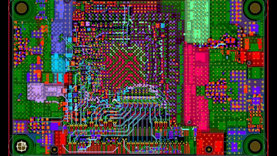
The genesis of any successful Printed Circuit Board (PCB) lies in a meticulously executed design process. This phase, preceding physical manufacturing, is critical for translating a conceptual idea into a functional, manufacturable board. It involves schematic capture, PCB layout, and careful consideration of materials, layer configuration, and component placement—all pivotal factors in achieving optimal manufacturing outcomes.
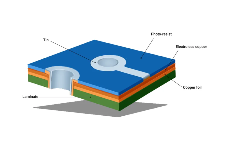
The transformation of a PCB design from digital blueprints into a tangible physical board involves a series of intricate fabrication steps. This section details these critical processes, ensuring that a design's intent is accurately materialized into the final PCB.
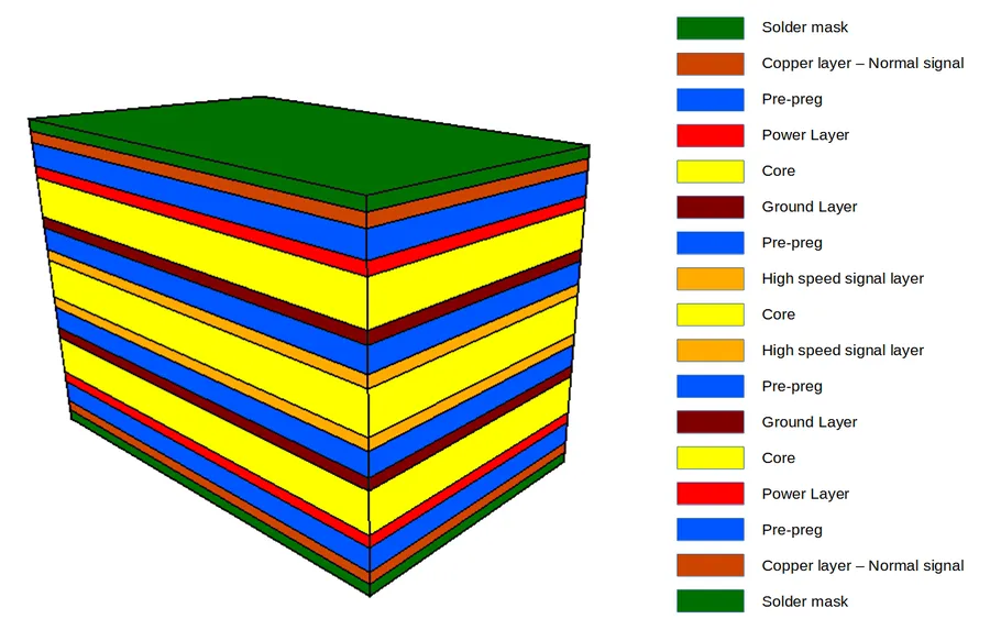
The creation of inner layers is a pivotal step in manufacturing multilayer PCBs, demanding meticulous control and precision. This process, specific to multilayer boards, involves a sequence of imaging, etching, and layering, crucial for building the functional complexity of modern electronics. These inner layers form the backbone of multilayer PCBs, providing electrical connectivity and signal routing within the board.
The process of inner layer production is technically complex and requires high precision, it ensures signal integrity and proper electrical function of the final product.
| Process Step | Description | Key Requirements |
|---|---|---|
| Imaging | Transferring the design onto copper clad laminate using photoresist and UV exposure. | High-resolution, accurate photo masks, controlled UV exposure. |
| Etching | Removing unwanted copper using chemical solutions after imaging. | Precise control of etching time and chemical concentration, uniform etching. |
| Layering | Stacking etched layers with prepreg, to build multilayer structure | Precise layer alignment and consistent bonding of layers |
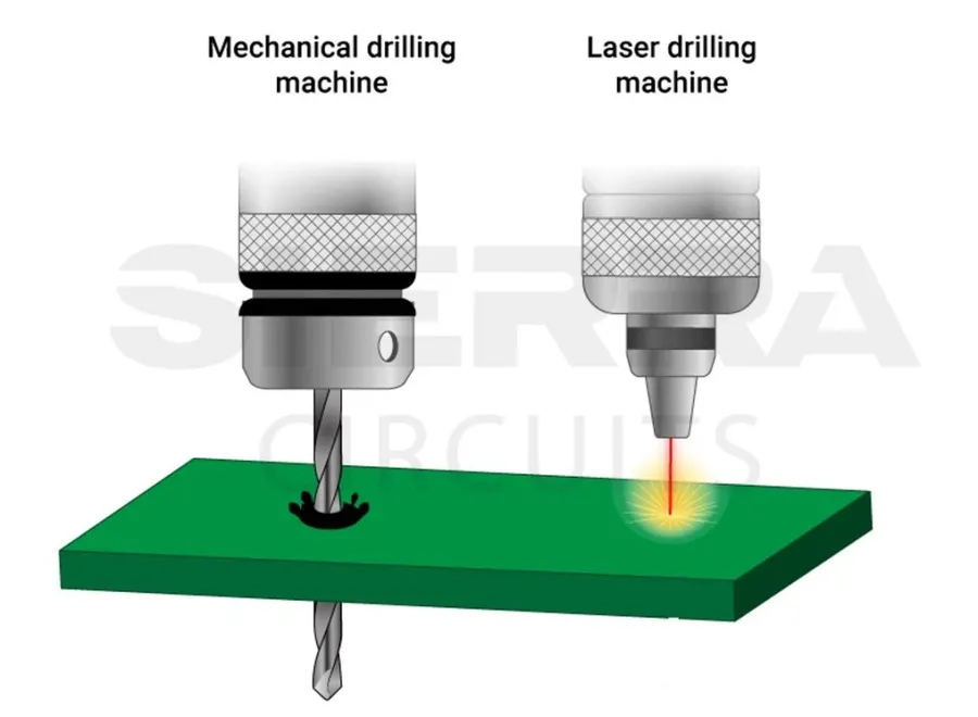
Following the etching process, the creation of electrical connections between different layers of a PCB requires precise drilling, plating, and layer bonding techniques. This stage is crucial in transforming individual layers into a fully functional, interconnected circuit board.
The following processes detail the methodologies employed in creating these vital interlayer connections.
| Process | Description | Purpose | Key Considerations |
|---|---|---|---|
| Precision Drilling | High-precision drilling machines create holes through the layers of the PCB. These holes are the foundation for vias and component mounting. | To establish precise paths for electrical connections and accommodate component leads. | Drill bit size, hole location accuracy, and material compatibility. |
| Electroless Plating | A thin layer of conductive material (typically copper) is deposited inside the drilled holes using a chemical process, creating a conductive base. | To enable subsequent electrolytic plating and create an initial conductive pathway. | Uniformity of plating, chemical concentration, and process temperature. |
| Electrolytic Plating | A thicker layer of copper is electroplated onto the electroless layer, strengthening the conductive pathway in the holes and on the surface. | To create robust and reliable connections through the drilled vias and enhance surface conductivity for the next steps. | Plating thickness control, current density, and bath chemistry. |
| Layer Bonding | Pre-etched, drilled and plated layers are stacked and pressed together under heat and pressure using a bonding adhesive (prepreg). | To create a solid, integrated multi-layer PCB with strong interlayer adhesion. | Alignment accuracy, bonding temperature, pressure, and prepreg material. |
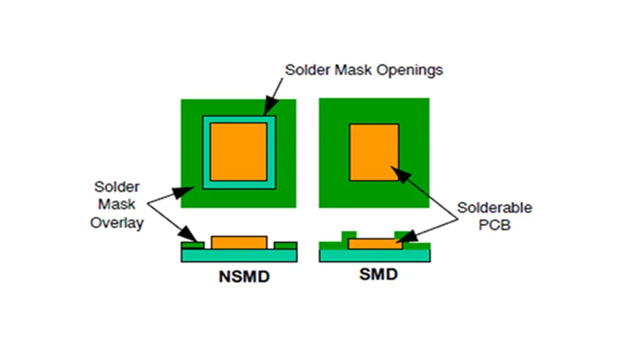
Soldermask and silkscreen applications are critical steps in PCB manufacturing, ensuring both the long-term reliability and ease of use of the final product. The soldermask acts as a protective layer, preventing shorts and corrosion, while the silkscreen provides vital component identification information, assisting during assembly and maintenance.
The application process is typically automated to ensure high precision and consistency across the PCB surface. These layers are not merely cosmetic but are fundamental to the functional longevity and serviceability of the circuit board.
| Feature | Soldermask | Silkscreen |
|---|---|---|
| Purpose | Protect copper traces from corrosion and electrical shorts | Provide component identification, polarity, and test points |
| Material | Polymer-based epoxy or similar material | Epoxy ink or UV curable ink |
| Color | Typically green, but can be other colors such as red, blue, black, and white | Typically white, but other colors are also available |
| Application | Applied after plating, before silkscreen | Applied after soldermask |
| Curing | Cured using heat or UV light | Cured using UV light or heat |
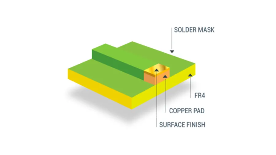
Surface finishing is a critical step in PCB manufacturing, directly impacting the board's solderability, resistance to corrosion, and overall reliability. The selection of the appropriate surface finish is crucial for optimal performance and longevity of the assembled PCB.
| Surface Finish | Description | Advantages | Disadvantages | Typical Applications |
|---|---|---|---|---|
| HASL (Hot Air Solder Leveling) | Molten solder is applied and then leveled with hot air knives. | Low cost, good solderability, widely available. | Uneven surface, not suitable for fine-pitch components, leaded (Pb) HASL is not RoHS compliant. | General purpose PCBs, through-hole and larger SMT components. |
| ENIG (Electroless Nickel Immersion Gold) | A layer of nickel is plated followed by a thin layer of immersion gold. | Excellent solderability, good corrosion resistance, flat surface for fine-pitch components, RoHS compliant. | Higher cost, black pad risk, not suitable for direct wire bonding. | Fine-pitch SMT components, wire bonding, high-reliability applications. |
| OSP (Organic Solderability Preservative) | A thin organic layer is applied to the copper surface to protect it from oxidation. | Low cost, flat surface, good solderability, RoHS compliant. | Short shelf life, sensitive to handling, may not withstand multiple reflow cycles. | Cost-sensitive applications, lower complexity designs, boards with few assembly cycles. |
| Immersion Tin | A thin layer of tin is deposited through chemical immersion. | Good solderability, flat surface, RoHS compliant. | Tin whiskers can be a reliability issue, sensitive to handling and storage. | Applications where moderate performance and cost is a factor. |
| Immersion Silver | A thin layer of silver is deposited through chemical immersion. | Excellent solderability, good conductivity, RoHS compliant | Susceptible to tarnishing, requires special storage to prevent oxidation. | High-frequency applications, switch contacts, or other applications which require high conductivity. |
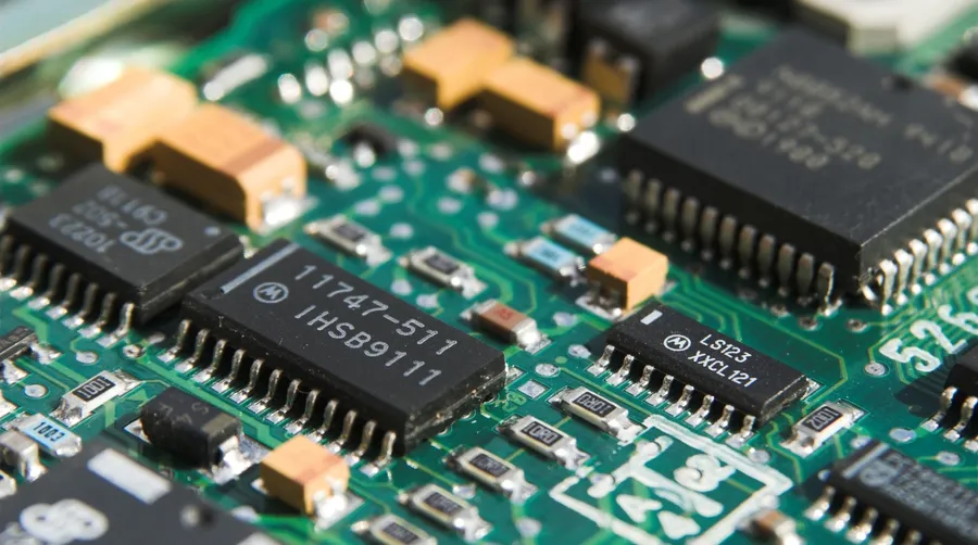
PCB assembly is the crucial stage where electronic components are precisely placed and soldered onto the fabricated printed circuit board, transforming it from a bare board into a functional electronic module. This process involves sophisticated techniques and equipment to ensure accurate placement and reliable electrical connections.
The assembly process can be broadly categorized into automated and manual methods, each suited for different production volumes and complexity levels.
| Method | Volume | Accuracy | Cost | Application |
|---|---|---|---|---|
| Automated Assembly | High | High | Lower per unit | Mass production, complex designs |
| Manual Assembly | Low | Variable (skilled labor required) | Higher per unit | Prototyping, low-volume runs, unique component requirements |
Regardless of the method, meticulous attention to detail and adherence to industry standards are essential to prevent defects and ensure the final product's reliability.
Rigorous quality control and testing are indispensable in PCB manufacturing to guarantee that the final product aligns with the stringent specifications required for reliable electronic performance. These processes are designed to detect and rectify any manufacturing defects, ensuring that each PCB operates as intended and meets the highest standards of reliability and longevity.
The testing phase involves multiple stages, from initial visual inspections to sophisticated electrical and functional tests. Each type of test serves a unique purpose, contributing to a comprehensive evaluation of the manufactured PCB.
Below are key quality control and testing methods used in PCB manufacturing:
These testing methods are crucial to ensure that the manufactured PCBs are ready for their intended applications and conform to the highest reliability standards, minimizing the risk of product failures, which can be costly and damaging to reputation.
This section addresses common questions regarding PCB manufacturing, providing clear and concise answers to enhance understanding of the processes involved in creating printed circuit boards.
Understanding the nuances of PCB manufacturing is essential for any electronics project. From meticulous design to precise fabrication, every step plays a crucial role in the final performance and reliability of the product. By choosing the right materials, processes, and manufacturer, you can ensure that your PCB is manufactured to the highest standards, resulting in a high-performing and durable electronic device. As technology advances, so too will the process of PCB manufacturing, always striving for better, smaller, and more efficient solutions.

