
In the high-stakes world of automotive electronics, a Transmission Control Unit (TCU) is only as reliable as its board. When facing the brutal combination of intense engine heat and relentless road vibration, standard PCB designs fail. This guide provides veteran engineering insights into DFM strategies that ensure your TCU designs stay operational under the most punishing conditions.
The Physics of Failure: Thermal Cycling and Vibration in TCUs
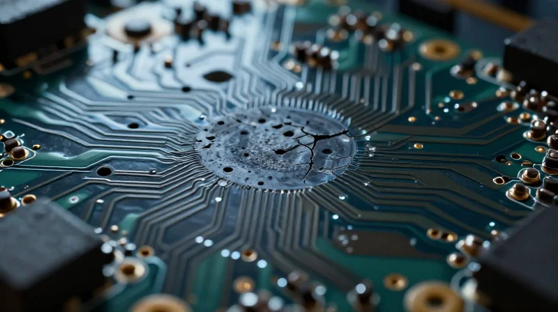
The Physics of Thermal Fatigue
The primary cause of failure in high-reliability TCU PCBs subjected to extreme thermal zones is the mismatch in the Coefficient of Thermal Expansion (CTE) between the copper traces, solder joints, and the dielectric substrate (typically FR-4). When a TCU undergoes rapid temperature transitions, the varying expansion rates induce shear stress at the interfaces. Over thousands of cycles, this stress leads to micro-cracking, barrel cracking in vias, and eventual delamination, which can result in intermittent electrical conductivity or total circuit failure.
Mechanical Stress and Vibration Resonance
TCUs mounted directly to transmission housings are exposed to high-frequency engine and road vibrations. If the PCB layout does not account for the natural frequency of the board, mechanical resonance can lead to fatigue fractures in solder interconnects, particularly in BGA (Ball Grid Array) packages. Designers must implement localized stiffening and optimize component placement to minimize parasitic mass and flexure.
Failure Mode Comparison
| Failure Mechanism | Primary Cause | Mitigation Strategy |
|---|---|---|
| Solder Joint Cracking | CTE Mismatch/Fatigue | Use high-reliability alloys or underfill |
| Via Barrel Cracking | Z-axis expansion stress | Increase copper plating thickness in holes |
| Substrate Delamination | Interfacial bond failure | Select high-Tg materials (Tg > 170C) |
Frequently Asked Questions on TCU Reliability
- Why does a higher Glass Transition Temperature (Tg) matter?
A higher Tg ensures the resin matrix remains stable at elevated temperatures, preventing the board from softening and reducing the rate of Z-axis expansion that breaks through-hole vias. - How does vibration affect component layout?
Large, heavy components should be placed near support points or mounting screws to minimize mechanical deflection; placing them in the center of a board increases the risk of fatigue due to displacement amplitude.
Material Selection: Beyond Standard FR-4
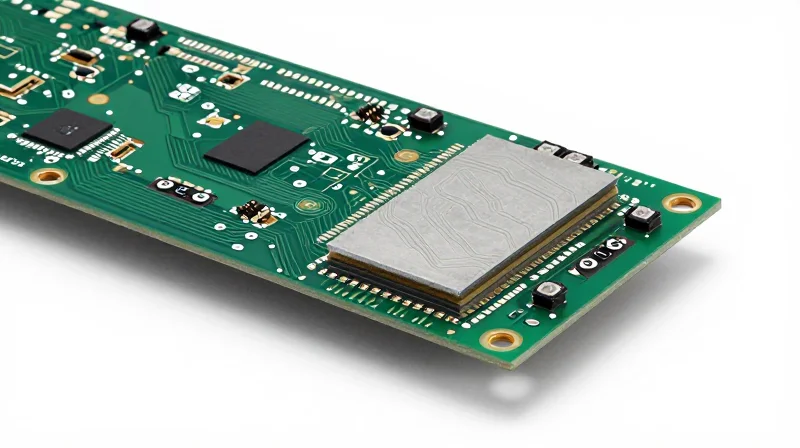
The Necessity of High-Tg and Low-CTE Substrates
Standard FR-4, with its typical Glass Transition Temperature (Tg) of 130°C to 140°C, is insufficient for automotive TCU environments where operational and ambient temperatures frequently push material limits. When a PCB exceeds its Tg, the resin matrix transitions from a glassy state to a rubbery state, causing the Coefficient of Thermal Expansion (CTE) to spike—often by a factor of three or four. This rapid expansion puts extreme mechanical stress on plated through-holes (PTHs) and internal copper traces. To ensure long-term survivability, engineers must specify high-Tg (170°C+) laminates that maintain structural integrity and a low CTE in the Z-axis, effectively minimizing the internal forces that lead to barrel cracking during extreme thermal cycling.
Material Performance Comparison
| Material Class | Typical Tg (°C) | Z-axis CTE (50-260°C) | Application Suitability |
|---|---|---|---|
| Standard FR-4 | 130-140 | 3.5-4.5% | Consumer Electronics (Low Risk) |
| High-Tg FR-4 | 170-180 | 2.5-3.0% | Industrial/Basic Automotive |
| Polyimide/Ceramic-Filled | 200-250+ | 1.0-1.8% | Extreme Thermal TCU/Aerospace |
Design Considerations for Extreme Environments
- Why is the Z-axis CTE more critical than the X/Y axes?
In a TCU, the Z-axis expansion is the primary driver of failure in plated through-holes. Because the board expands faster than the copper barrels, it exerts a 'pulling' force that leads to circumferential fatigue cracks in the hole walls. - How does ceramic-filled resin improve reliability?
Ceramic fillers are inert and have an extremely low CTE. By incorporating them into the epoxy resin, the overall bulk CTE of the dielectric is reduced, significantly narrowing the mismatch between the PCB substrate and the copper circuitry. - Should I consider metal-backed (IMS) boards?
For high-power components within the TCU, Insulated Metal Substrates (IMS) offer superior thermal dissipation. However, they must be matched with compatible thermal interface materials to prevent mechanical decoupling during temperature shifts.
Optimizing Layer Stack-up for Structural Integrity
For Transmission Control Units (TCUs), structural integrity is fundamentally tied to the symmetry and material balance of the PCB stack-up. In extreme thermal environments, mismatched expansion coefficients or asymmetrical copper distributions act as primary drivers for board warping, delamination, and subsequent solder joint fatigue. Achieving long-term reliability requires a rigorous approach to balance forces across the Z-axis during both manufacturing reflow and end-use thermal oscillation.
The Importance of Mechanical Symmetry
Mechanical symmetry is the cornerstone of a warp-resistant design. An asymmetric stack-up—where copper density or core thickness varies significantly between the top and bottom halves of the board—creates uneven internal stresses. As the board heats up, these imbalances manifest as physical deformation. Designers must ensure that copper weight distribution is mirrored across the neutral axis of the PCB.
| Design Element | Risk if Improperly Balanced | Reliability Mitigation Strategy |
|---|---|---|
| Copper Weight | Bowing and Twisting | Distribute copper planes evenly across both signal layers and planes |
| Core Thickness | Z-axis Expansion Stress | Utilize symmetrical core/prepreg layouts around the center layer |
| Via Placement | Localized Delamination | Stagger heavy via arrays to prevent concentrated mechanical tension |
DFM Guidelines for Layer Stack-up
- Why is layer symmetry critical for TCU boards?
Symmetry ensures that thermal expansion forces remain uniform across the PCB cross-section. If the top side expands faster than the bottom due to copper imbalance, the board will experience internal torque, leading to permanent bowing. - How does copper weight affect thermal stability?
Heavy copper layers provide excellent heat dissipation but introduce significant stiffness. If high-weight copper is not balanced by an identical layer on the opposite side, the PCB will act as a bimetallic strip when subjected to temperature extremes. - What role does core thickness play in warp resistance?
Using identical core thicknesses for mirrored layers ensures that the modulus of elasticity remains consistent, which minimizes localized internal stress concentrations during the glass transition temperature (Tg) crossover.
To further optimize for reliability, adhere to the 80/20 rule: aim for copper coverage variance of less than 20% across mirrored signal layers. When working with high-density interconnects (HDI), prioritize sequential buildup processes that maintain symmetry at every lamination stage, rather than forcing a complex asymmetric stack.
Via Reliability: Techniques for High-Vibration Environments
In extreme vibration environments, the via barrel acts as a primary failure point due to repetitive stress cycles induced by coefficient of thermal expansion (CTE) mismatches. Ensuring reliability requires moving beyond standard manufacturing tolerances to prioritize structural ductility and stress dissipation.
Critical Via Design Parameters
| Design Parameter | Recommended Standard | Rationale for Reliability |
|---|---|---|
| Aspect Ratio | Maximum 6:1 | Reduces plating stress in deep, narrow holes. |
| Barrel Plating | 25 µm (minimum) | Prevents premature barrel thinning and cracking. |
| Via Diameter | >0.3 mm | Allows for more uniform electrolytic plating deposition. |
Reinforcement Techniques for Mechanical Integrity
To mitigate crack propagation, designers should implement targeted reinforcement strategies. The use of 'tear-drop' pads is essential to improve the transition between the via barrel and the copper trace, which reduces localized stress concentrations during vibration. Furthermore, avoiding the placement of vias within the direct path of high-vibration stress, such as near heavy components or mounting holes, remains a critical layout discipline.
FAQ: Via Reliability and Best Practices
- Why is copper plating thickness crucial?
Thin plating creates high-stress points during thermal expansion; a minimum of 25 micrometers ensures that the barrel can withstand mechanical strain without fracturing. - How does aspect ratio affect vibration endurance?
Higher aspect ratios often lead to inconsistent plating distribution. Keeping the ratio at 6:1 or lower ensures structural uniformity along the entire depth of the barrel. - Should I use microvias in vibration-prone zones?
Microvias are highly susceptible to fatigue; for extreme environments, through-hole vias with robust plating are significantly more reliable.
Solder Joint Integrity and Component Placement
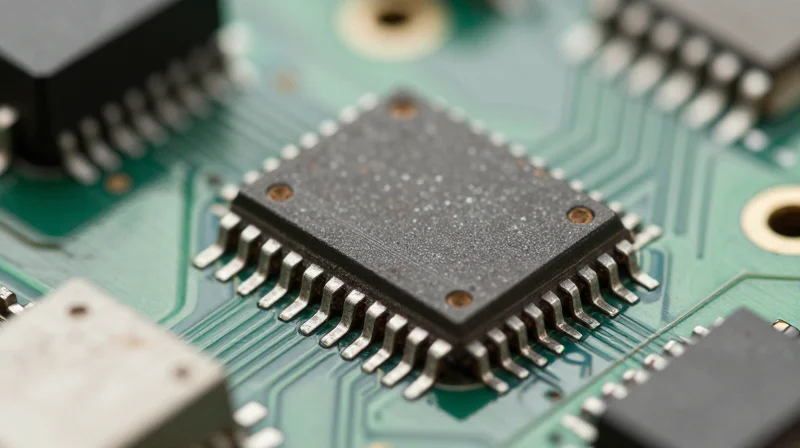
Mitigating Thermomechanical Stress on BGA and QFN Packages
In TCU applications exposed to extreme thermal cycling, the coefficient of thermal expansion (CTE) mismatch between the PCB substrate and component packages remains the primary driver of solder joint fatigue. To mitigate failure, engineers must prioritize trace routing that avoids stress concentrations at component corners and implement thermal relief patterns that accommodate differential expansion without inducing parasitic inductance.
| Failure Driver | Design Mitigation Strategy | Resulting Benefit |
|---|---|---|
| CTE Mismatch | Match substrate CTE to package | Reduced shear strain |
| Component Warpage | Optimized pad geometry | Improved joint ductility |
| Vibration Fatigue | Underfill encapsulation | Load distribution |
Strategic Component Placement and Underfill Protocols
Placement density should favor thermal isolation. High-power components must be positioned to prevent localized thermal gradients. Furthermore, for BGA and QFN packages subjected to persistent vibration, capillary or jet-dispensed underfills are mandatory to redistribute mechanical stress from the solder joints to the PCB surface.
- Why is component orientation critical in high-thermal zones?
Proper orientation minimizes the bending moment on solder balls during board flexing, ensuring that the primary axis of package thermal expansion aligns with the layout to prevent shear failure. - When is underfill essential for QFN packages?
Underfill is essential whenever the application environment involves thermal cycling between -40°C and +125°C or high-frequency vibration, as it anchors the component to the board, preventing fatigue cracking at the solder interface. - Does pad design impact solder joint reliability?
Yes, utilizing solder mask defined (SMD) pads for smaller BGAs provides superior mechanical anchoring compared to non-solder mask defined (NSMD) pads in high-vibration applications.
Design Guidelines for Solder Reliability
# Best practices for DFM in extreme thermal TCU zones
- Pad Sizing: Maintain 1:1 pad-to-ball ratio for BGAs.
- Symmetry: Ensure thermal vias are balanced to avoid package tilt.
- Underfill: Specify high-Tg capillary flow material for QFNs.
- Clearance: Allow minimum 1.5mm keep-out for underfill fillet.
Thermal Management and Heat Dissipation Design

Core Strategies for Thermal Dissipation
Thermal management in Transmission Control Units (TCUs) is not merely about temperature reduction but about maintaining the junction temperatures of power electronics within safe operating margins during peak transient loads. A robust DFM strategy focuses on creating low-impedance thermal paths from the component silicon to the ambient environment, utilizing PCB features such as thermal vias, extensive copper pours, and integrated heat sinking solutions.
| Technique | Primary Function | DFM Consideration |
|---|---|---|
| Thermal Vias | Vertical heat transfer | Ensure secondary plating; avoid solder wicking |
| Copper Pours | Lateral heat spreading | Maintain clear thermal relief for soldering |
| Embedded Heatsinks | Bulk heat extraction | Coefficient of thermal expansion (CTE) matching |
Optimizing Thermal Via Arrays
Thermal vias serve as the primary conduits for heat moving from the component side to the inner copper planes or the bottom side of the TCU. To maximize efficacy, engineers must design for high-density stitching patterns under power-dense packages like MOSFETs. It is crucial to specify small-diameter, copper-plated holes that minimize drilling complexity while maximizing surface area for thermal conductivity.
Frequently Asked Questions
- Should thermal vias be plugged or filled?
For high-reliability TCUs, conductive epoxy filling is recommended to prevent solder wicking and ensure structural integrity during assembly, which also improves thermal performance. - How much copper is required for effective heat spreading?
Internal planes should utilize at least 2oz copper weight to facilitate lateral heat dissipation, ensuring that the thermal bottleneck at the component footprint is effectively relieved. - Does component placement impact thermal management?
Yes, high-heat dissipating components must be isolated from temperature-sensitive sensors to prevent thermal cross-talk and drift in critical calibration data.
Signal Integrity (SI) under Thermal Stress
Managing Impedance Stability under Thermal Variance
Signal integrity in Telematics Control Units (TCUs) is intrinsically linked to the dielectric constant (Dk) of the substrate material. As temperatures fluctuate in extreme environments, the polymer matrix of the PCB dielectric undergoes physical expansion and molecular shifts, causing the Dk to drift. This fluctuation directly alters the characteristic impedance of high-speed transmission lines, leading to signal reflections, increased insertion loss, and data corruption.
| Parameter | Effect of Heat | Design Mitigation |
|---|---|---|
| Dielectric Constant (Dk) | Increases with Temperature | Select Low-Dk-Thermal-Coefficient Laminates |
| Copper Resistance | Increases Linearly | Optimize Trace Widths for Thermal Headroom |
| Insertion Loss | Increases due to Df Changes | Utilize Low-Loss, High-Tg Materials |
Strategies for Consistent Signal Propagation
To maintain signal integrity, designers must account for these environmental variables during the layout phase. Using materials with a low Dk-Thermal Coefficient (TCDk) is the most effective approach to minimizing impedance variation. Furthermore, calculating the 'worst-case' impedance shift during the signal integrity simulation phase ensures that designs remain within acceptable eye-diagram margins even at maximum operating temperatures.
- How does Dk shift affect differential pairs?
Thermal Dk drift creates phase skew and impedance mismatch between legs of a differential pair, which degrades the common-mode rejection ratio and increases electromagnetic interference. - What material properties are critical for TCUs?
Prioritize materials with a high Glass Transition Temperature (Tg) and a low Coefficient of Thermal Expansion (CTE) in the Z-axis to prevent via barrel fatigue alongside stable electrical performance. - Is simulation enough to guarantee performance?
Simulations must include temperature-dependent material models rather than nominal values to capture the true behavior of the PCB in extreme thermal zones.
DFM Verification and Testing Protocols
Validation Through Accelerated Life Testing
For TCU designs destined for extreme thermal zones, standard burn-in testing is insufficient. Engineers must employ Highly Accelerated Life Testing (HALT) and Highly Accelerated Stress Screening (HASS) to expose latent design weaknesses in manufacturing and assembly. By subjecting prototypes to rapid thermal cycling and vibration simultaneously, manufacturers can identify failure points—such as PCB delamination or interconnect fracture—long before the unit reaches the field.
Comparison of Thermal Stress Verification Methods
| Method | Primary Goal | Application Stage |
|---|---|---|
| HALT | Identify design robustness limits | Prototype/Design Phase |
| HASS | Detect manufacturing defects | Production/Screening Phase |
| Thermal Shock | Validate solder joint resilience | Qualification Testing |
DFM Verification Protocols and FAQ
- How does HALT validate DFM choices?
HALT forces the design beyond standard specifications, allowing engineers to verify if specific DFM features like copper weight, thermal via density, and solder mask bridges perform as modeled under fatigue. - Why is cross-sectional analysis vital?
Post-stress testing, destructive cross-sectional analysis confirms whether internal structures, particularly micro-via integrity and barrel plating thickness, have maintained structural stability. - What is the role of the 'Golden Board' in testing?
The 'Golden Board' serves as the baseline reference for HASS, ensuring that variations in manufacturing yield do not mask thermal stress failures in mass production.
Implementing a rigorous testing protocol ensures that the DFM strategy for TCU PCBs transitions successfully from the virtual design environment to the physical rigors of the engine compartment or transmission housing. Consistent failure analysis feedback loops must be integrated into the DFM cycle to iterate and refine board architecture.
Designing for extreme environments requires a proactive approach that prioritizes structural integrity alongside electrical performance. By implementing these rigorous DFM standards, you can reduce field failures and ensure your TCU hardware delivers consistent performance. Ready to optimize your next project? Contact our engineering team today for a comprehensive DFM audit.
