
In the world of medical wearables, space is the ultimate luxury. Designing ultra-miniature flexible PCBs for next-generation hearing aids requires a shift from traditional engineering to high-precision manufacturing discipline. We address the technical barriers that often lead to assembly failure and guide you through the DFM strategies required for peak reliability.
The Challenge of Miniaturization in Hearing Aid Design

The Physical Constraint Paradigm
The primary challenge in hearing aid miniaturization is the radical reduction of internal volume while maintaining or increasing processing power. Engineers must manage complex routing density on substrates often smaller than a fingernail, necessitating high-density interconnect (HDI) technologies. This compression forces a departure from standard PCB practices, requiring a deep understanding of layer stack-ups, micro-vias, and buried components to accommodate advanced digital signal processing (DSP) chips and wireless transceivers.
Comparative Design Constraints
| Parameter | Standard Consumer PCB | Ultra-Miniature Hearing Aid PCB |
|---|---|---|
| Via Technology | Through-hole | Laser-drilled Micro-vias |
| Trace/Space | 4-6 mil | Under 2 mil |
| Component Pitch | 0.5mm - 0.8mm | 0.2mm - 0.3mm (01005 chips) |
| Layer Density | 4-6 Layers | 8-12+ HDI Layers |
Common DFM Challenges and Mitigation
- How does miniaturization impact thermal management?
Smaller form factors drastically limit heat dissipation pathways. DFM strategies must prioritize low-power components and strategic copper pouring to act as heat sinks without violating clearance rules. - What role do micro-vias play in reliability?
As boards shrink, micro-vias replace traditional vias to save space, but they introduce higher risk of barrel cracking during reflow. Ensuring optimized pad-to-drill alignment is critical. - Why is signal integrity harder in small boards?
Increased density causes tighter coupling between traces, leading to cross-talk. Shielding layers and strictly controlled dielectric constants become essential for high-frequency wireless performance.
Flexible PCB Material Selection and Bend Radius Considerations
Material Selection for Dynamic Flexure
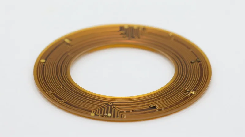
In hearing aid manufacturing, the substrate choice determines both the durability and the minimum form factor of the assembly. Polyimide (PI) remains the industry standard due to its exceptional thermal stability and mechanical flexibility. However, for ultra-miniature designs requiring extreme curvature, engineers must differentiate between adhesiveless polyimide laminates and those with adhesive layers.
| Material Type | Flexibility | Best Use Case |
|---|---|---|
| Adhesiveless PI | High | Dynamic flexing in ultra-thin devices |
| Adhesive-based PI | Moderate | Static bends or less constrained routing |
| Modified Polyimide | Very High | Complex 3D folding and high-density interconnects |
Calculating Minimum Bend Radius
Exceeding the mechanical limits of a flexible circuit leads to copper work-hardening and inevitable fatigue failure. The general rule of thumb for dynamic flex circuits is a bend radius of at least 10 to 12 times the total circuit thickness. For static applications, this can be reduced, but for hearing aids where the device undergoes daily insertion and removal stress, following a conservative safety margin is non-negotiable.
Frequently Asked Questions
- How does copper grain structure impact flex life?
Always specify Rolled Annealed (RA) copper for dynamic applications; its horizontal grain structure is significantly more resistant to crack propagation during repeated bending compared to Electro-Deposited (ED) copper. - Can I use stiffeners in flexible areas?
Stiffeners are used to support component mounting sites; however, ensure there is a clear mechanical transition zone (the 'bend relief' area) to prevent stress concentrations at the edge of the stiffener. - Why does trace width matter in bends?
Narrower traces positioned in the neutral axis of the bend experience less compressive or tensile stress, significantly increasing the cycle life of the trace during repeated flexion.
Optimizing High-Density SMT Component Placement
Optimizing High-Density SMT Component Placement
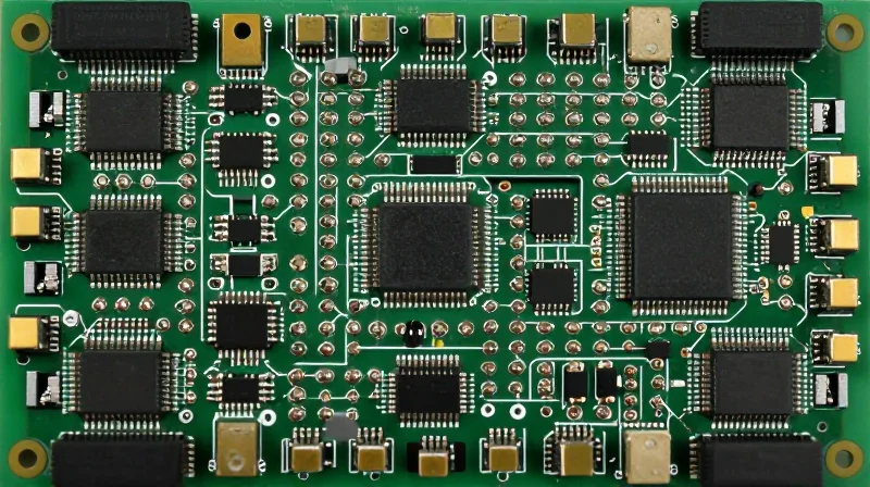
In ultra-miniature PCB design, such as those found in modern hearing aids, component density frequently pushes the boundaries of standard assembly capabilities. Achieving reliable solder joints in these confined spaces requires a transition from traditional manual layout methods to algorithmic optimization. The primary strategy involves minimizing thermal mass disparities and ensuring adequate spacing for solder stencil deposition to prevent bridging, which is common with 01005 or smaller components.
Strategic Placement Guidelines for Miniature Assemblies
To achieve high-yield production, designers must prioritize placement orientation relative to the reflow process and stencil aperture constraints. Components should be oriented to ensure that solder paste flow is uniform across the pads during the reflow stage, effectively preventing 'tombstoning' or cold joints.
| Parameter | High-Density Recommendation | Reliability Impact |
|---|---|---|
| Component Orientation | Aligned with reflow wave | Reduces tombstoning risks |
| Pad-to-Pad Spacing | Minimum 100 microns | Limits solder bridge defects |
| Thermal Vias | Staggered array patterns | Improves heat dissipation |
- How do you manage solder paste volume at extreme densities?
Utilize laser-cut electroformed stencils with precisely calculated aperture-to-pad ratios, ensuring that paste volume is consistent and sufficient without causing solder balling. - What is the critical spacing for 01005 components?
While IPC standards vary, a minimum of 0.1mm clearance is recommended for high-reliability hearing aid devices to accommodate pick-and-place accuracy tolerances.
Maintaining Signal Integrity in Ultra-Compact Layers

Mitigating Crosstalk in High-Density Interconnects
In the confined space of a hearing aid, proximity-induced crosstalk is the primary enemy of signal fidelity. As trace density increases, capacitive and inductive coupling between adjacent nets can distort high-frequency audio paths. Engineers must prioritize differential pair routing, maintaining strict impedance control, and utilizing guard traces or increased spacing where physical constraints permit to minimize electromagnetic interference.
Comparison of EMI Mitigation Strategies
| Strategy | Effectiveness | Design Trade-off |
|---|---|---|
| Differential Routing | High | Requires matching trace lengths |
| Guard Traces | Medium | Consumes valuable real estate |
| Ground Plane Stitching | Very High | Increases layer count |
Stack-Up Design for Signal Isolation
The vertical architecture of the PCB is critical for noise suppression. Implementing a dedicated ground plane adjacent to high-speed signal layers creates a low-impedance return path, which is essential for reducing loop area and radiating EMI. For complex multi-layer designs, using micro-vias allows for clean layer transitions without creating long stubs that act as unintentional antennas.
Common Signal Integrity Challenges
- How do trace stubs impact audio signal quality?
Unterminated stubs create reflections that manifest as jitter, causing harmonic distortion in the audio signal; they should be avoided or removed via back-drilling where feasible. - Is via-in-pad technology risky for signal integrity?
While it optimizes density, via-in-pad can create parasitic inductance; ensure vias are properly filled and capped to maintain a smooth surface for SMT components. - What is the impact of flexible circuit bending on impedance?
Repeated mechanical stress on flexible layers can lead to micro-cracks in traces, altering their impedance and potentially causing signal intermittent failure.
Advanced Thermal Management Strategies

Advanced Thermal Management Strategies
In the confined environment of a hearing aid, thermal management is not merely a reliability concern but a patient safety requirement. As processing power increases, the heat density within sub-cubic-centimeter enclosures can lead to skin irritation or accelerated component degradation. Advanced DFM strategies focus on maximizing the thermal conductivity of the PCB assembly itself to serve as a passive heat spreader, effectively leveraging the device chassis to dissipate heat away from critical ICs.
Passive Heat Dissipation Techniques
For miniature electronics, we utilize high-thermal-conductivity substrates and strategic copper utilization. By integrating thermal vias directly under high-power DSP chips, we create a low-resistance path to internal ground planes, which act as a distributed heat sink.
| Strategy | Mechanism | Effectiveness |
|---|---|---|
| Thermal Vias | Connects hotspots to internal ground planes | High |
| Copper Pouring | Increases total thermal mass | Medium |
| Thermal Gap Pads | Bridges gap between IC and chassis | Extreme |
Frequently Asked Questions
- How do thermal vias impact signal integrity?
While essential for cooling, dense via arrays must be carefully placed to avoid creating discontinuous ground return paths or parasitic inductance that could interfere with high-speed signal traces. - Can flexible PCBs aid in thermal management?
Yes, polyimide flexible substrates can be bonded to rigid heat-conducting stiffeners, allowing the flex section to transport heat from the components to a larger, cooler area of the device housing. - Is active cooling feasible in hearing aids?
No, the space constraints and power limitations make active cooling (fans or pumps) impossible; therefore, passive conduction paths remain the only viable approach.
DFM Standards for Automated Assembly
Establishing DFM Standards for Automated Assembly
For hearing aid assemblies, the transition from prototype to high-volume automated production necessitates a strict alignment with SMT (Surface Mount Technology) equipment capabilities. Even when using bespoke flexible circuits, designers must incorporate rigid tooling strips, precise fiducial markers, and standardized panelization to prevent mechanical jamming and ensure consistent component placement accuracy.
Critical DFM Parameters for Miniature PCB Automation
| Parameter | Design Rule | Reasoning |
|---|---|---|
| Panel Rails | 5mm minimum width | Required for conveyor stability |
| Fiducials | 3-point global + local | Ensures sub-micron placement accuracy |
| Component Pitch | Minimum 0.15mm gap | Prevents solder bridging at volume |
| Edge Clearance | 1mm buffer from routing | Prevents trace damage during singulation |
Frequently Asked Questions
- Why are rigid tooling strips mandatory for flexible circuits?
Flexible materials lack the structural rigidity required for automated SMT lines. Applying temporary rigid stiffeners allows the assembly equipment to transport, clamp, and register the PCB as if it were a standard rigid board. - How do we handle fiducial placement on ultra-dense boards?
Prioritize global fiducials on the panel rails and local fiducials adjacent to fine-pitch components (like micro-BGAs). Ensure high-contrast solder mask clearance around these marks to guarantee recognition by vision systems. - What is the biggest risk during automated singulation?
Mechanical stress during the breaking or routing of the PCB from the panel. Proper DFM dictates using small tab routing with 'mouse bites' to minimize vibration transfer to delicate solder joints.
Overcoming Common Manufacturing Pitfalls

Strategies for Mitigating Miniature PCB Manufacturing Pitfalls
In the realm of ultra-miniature hearing aid electronics, the margin for error is nearly non-existent. Overcoming common pitfalls requires a proactive shift from reactive troubleshooting to predictive design-for-manufacturing (DFM) strategies that anticipate the high-stress nature of sub-millimeter component placement.
| Common Defect | Primary Root Cause | DFM Mitigation Strategy |
|---|---|---|
| Solder Bridging | Excessive solder paste deposition | Optimize aperture ratios and stencil thickness |
| Tombstoning | Imbalanced thermal mass on pads | Use thermal relief patterns to equalize heat |
| Trace Delamination | High localized thermal stress | Select high-Tg laminates and polyimide substrates |
Frequently Asked Questions on Assembly Reliability
- How can I prevent tombstoning on 01005 or smaller components?
Tombstoning often occurs due to uneven wetting forces. Ensure your design uses identical pad sizes and equalized trace widths to balance thermal dissipation during reflow, allowing both sides of the component to melt simultaneously. - Why does trace delamination occur frequently in flexible circuits?
It is usually caused by excessive heat exposure during rework or mismatched coefficients of thermal expansion (CTE). Ensure proper adhesion promoters are specified and limit peak reflow temperatures to the absolute minimum required for the solder alloy. - Is solder bridging strictly an assembly process issue?
While often blamed on the SMT line, bridging is frequently a design artifact. Ensure that solder mask dams are correctly defined between pads; if the gap is too small for manufacturing tolerances, adjust pad footprint geometry to reduce overlap area.
By adhering to rigorous DFM protocols and focusing on thermal equilibrium, engineers can successfully navigate the complexities of hearing aid miniaturization, ensuring both high yields and long-term device performance.
Collaborating with Your PCB Assembly Partner
In the world of ultra-miniature electronics, DFM is not a static set of rules but a dynamic conversation between the design team and the assembly house. Engaging your manufacturing partner early in the prototype phase is the single most effective way to avoid costly re-spins and yield degradation.
Early Engagement Strategies
For miniature hearing aid PCBs, design constraints often push the absolute limits of current manufacturing capabilities. Inviting your assembler to review your design during the schematic and layout phase—long before the Gerber files are finalized—allows them to flag potential bottlenecks that are invisible to design engineers.
- Why is early involvement crucial?
Early review prevents design choices that might be technically possible in CAD but yield-prohibitive in mass production, such as non-standard trace clearances or irregular solder mask openings. - How do you define manufacturing limits?
Establish a clear 'Capabilities Matrix' with your partner, documenting the minimum solder pad dimensions and registration tolerances they can consistently achieve on flex-rigid substrates. - What documentation is required?
Provide detailed stack-up definitions, controlled impedance requirements, and specific instructions for handling micro-miniature components like 008004 chip resistors.
Comparison: Standard vs. Miniature DFM Collaboration
| Feature | Standard PCBA | Hearing Aid/Ultra-Miniature |
|---|---|---|
| Design Review Timing | Post-Layout | Concept & Schematic Phase |
| Tolerance Buffers | Standard Industry Defaults | Sub-micron/Tight Process Control |
| Tooling Engagement | Standard Pallets | Custom Miniature Assembly Jigs |
| Feedback Cycle | Transactional | Iterative/Collaborative |
Optimizing Data Exchange and Validation
The integrity of your data package directly dictates the speed of the NPI (New Product Introduction) cycle. For hearing aid technology, standard DFM reports are often insufficient. Demand a 'Manufacturing Feasibility Report' from your partner that specifically addresses solder volume calculations and paste stencil design for your specific miniaturized pad geometry.
Successfully engineering ultra-miniature flexible PCBs for hearing aids demands a rigorous approach to DFM and a deep understanding of high-density assembly physics. By prioritizing these design pillars, you can reduce manufacturing iterations and accelerate time-to-market. Contact our engineering team today to discuss your next high-density PCB project and ensure your design is ready for large-scale production.
