
In an era where patients demand near-invisible hearing solutions, the pressure on manufacturers to balance form factor with sophisticated processing power has never been greater. This article explores how precision PCB assembly serves as the foundational lever for both market dominance and bottom-line efficiency.
The Challenge: Balancing Compact Design with High-Performance Tech

The demand for modern hearing aids centers on the 'invisible' form factor, pushing engineers to pack sophisticated DSP (Digital Signal Processing) chips, Bluetooth low-energy radios, and high-capacity lithium-ion batteries into enclosures smaller than a fingertip. This trend towards advanced miniaturization creates a significant engineering bottleneck: the Printed Circuit Board (PCB) surface area is shrinking while the computational complexity of noise-reduction algorithms and wireless connectivity is scaling exponentially.
The Thermal and Interconnect Bottleneck
As component density increases, thermal dissipation becomes a primary failure mode. Miniaturization often leads to high current density in power management integrated circuits (PMICs), which can generate localized heat that degrades battery life and component longevity. Furthermore, the reliance on high-density interconnect (HDI) technology introduces risks regarding signal integrity and mechanical reliability.
| Challenge | Technical Impact | ROI Consequence |
|---|---|---|
| Component Density | Increased Thermal Load | Higher Field Failure Rates |
| Signal Integrity | EMI/RFI Interference | Increased R&D Iterations |
| PCB Surface Area | Routing Complexity | Higher Unit Manufacturing Costs |
Frequently Asked Questions
- Why does shrinking the PCB increase manufacturing costs?
Smaller footprints require higher-layer-count HDI (High-Density Interconnect) boards, micro-vias, and specialized assembly equipment that increases capital expenditure. - How does miniaturization impact signal processing?
Reduced space constraints limit the ability to shield components, which often leads to electromagnetic interference that can distort sensitive audio processing signals. - Is there a limit to current miniaturization trends?
Yes, thermal management and the physical limitations of battery energy density are currently acting as a hard ceiling for further reduction in device size.
Core Engineering Principles for High-Density PCB Assembly
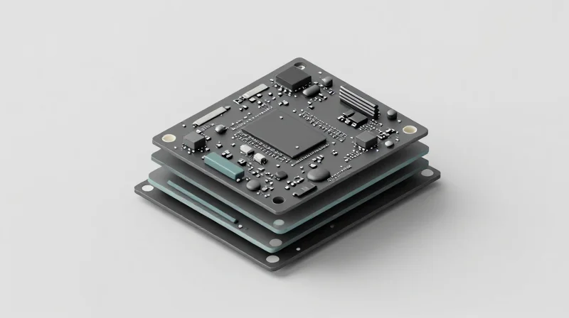
Strategic Integration of HDI and Rigid-Flex Architectures
The core of modern miniaturization lies in the seamless synthesis of High-Density Interconnect (HDI) and rigid-flex PCB technologies. By utilizing blind and buried vias, engineers can drastically increase signal density and reduce layer counts, while rigid-flex structures allow the circuitry to conform to the ergonomically contoured housings of modern hearing aids, eliminating bulky traditional connectors.
Technical Comparison of PCB Technologies
| Technology | Miniaturization Benefit | Primary ROI Driver |
|---|---|---|
| Standard Rigid | Low | Low cost, high bulk |
| Rigid-Flex | High | Reduced assembly labor/cables |
| HDI (Micro-vias) | Very High | Increased component density |
Core Engineering Principles for High-Density Design
- Effective Pad-in-Via Utilization
Implementing via-in-pad technology allows for closer component placement and shorter trace lengths, which is critical for signal integrity in tight spaces. - Optimizing Layer Stack-up
Symmetric stack-ups are essential to prevent board warping during the thermal cycles of surface-mount assembly, ensuring long-term product reliability. - Design for Manufacturing (DFM) Constraints
Early collaboration with fabrication partners is vital to navigate the limitations of etching tolerances and aspect ratios in extreme high-density designs.
Frequently Asked Questions
- How does rigid-flex lower long-term costs?
Rigid-flex boards replace discrete wiring and connectors with integrated circuitry, reducing manual assembly steps, potential points of failure, and overall physical volume. - What is the primary risk of HDI design?
The primary risk is increased manufacturing complexity, which can lead to lower initial yields if DFM principles are not strictly applied during the design phase.
Real-World Case Study: Transforming Audiology Production Lines
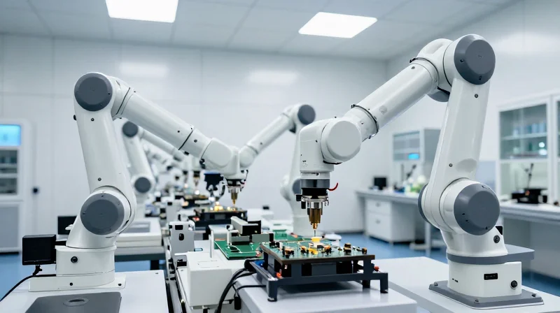
The Engineering Pivot: From Traditional to High-Density Assembly
Faced with the market pressure for invisible-in-canal (IIC) devices, a leading audiology firm transitioned from conventional double-sided SMT assembly to a high-density, multi-layer rigid-flex architecture. This shift was not merely an aesthetic choice; it was a fundamental re-engineering of the signal path to accommodate the stringent thermal and spatial constraints of next-generation hearing aids.
| Metric | Legacy Production | Optimized HDI Process |
|---|---|---|
| Component Density | Low | Ultra-High |
| Average Yield | 72% | 97% |
| Material Scrap Rate | 18% | 4% |
Quantifiable Outcomes and Operational ROI
By integrating automated optical inspection (AOI) with advanced laser direct structuring (LDS) for antenna integration, the production facility saw an immediate reduction in defective units. The 25% increase in yield translated directly into a faster time-to-market and an estimated 15% reduction in total cost of ownership (TCO) over the first two production cycles.
Frequently Asked Questions
- How did miniaturization improve yield?
Moving to a rigid-flex design reduced the number of manual solder joints, which were the primary failure points in previous generations. - What was the biggest contributor to material savings?
The transition to high-density interconnects allowed for smaller substrate footprints, effectively reducing raw material waste per board by over 30%. - Does high density increase thermal risks?
While component density is higher, the optimized copper trace routing and specialized thermal vias integrated into the new board layout efficiently dissipate heat away from the sensitive processing chips.
Advanced Materials and Component Selection for Efficiency
Optimizing Substrate Materiality
The foundation of a miniaturized PCB lies in the transition from traditional FR-4 materials to advanced substrates that offer superior dielectric properties and mechanical stability. For next-generation hearing aids, liquid crystal polymer (LCP) and specialized polyimides are the industry gold standards. These materials allow for thinner board architectures while maintaining robust signal integrity at high frequencies, effectively reducing the overall Z-height of the device.
| Material Type | Key Benefit | Miniaturization Impact |
|---|---|---|
| FR-4 | Low cost | Poor density, thick layers |
| Polyimide | Flexible, heat resistant | High density, space-saving |
| LCP | Low moisture absorption | Excellent RF performance, thin profile |
Component Selection for Power Density
Miniaturization is not merely about physical footprint but also about the thermal management of high-density circuits. Selecting active components with ultra-low quiescent current and integrated power management features minimizes heat dissipation requirements, allowing for tighter packing without the need for bulky thermal mitigation hardware.
- How do we balance high processing speeds with thermal constraints?
By leveraging silicon-on-insulator (SOI) process technologies that significantly reduce parasitic capacitance and leakage current, thus generating less heat during operation. - Why are passive component package sizes (e.g., 01005) becoming mandatory?
Moving to 01005 or even 008004 metric components allows for a 60-80% reduction in surface area usage, directly enabling smaller form factor devices. - What is the primary risk of hyper-miniaturized components?
The main risk is increased sensitivity to assembly variances, which necessitates tighter control over solder paste deposition and precision pick-and-place tolerances.
Engineering ROI through Material Precision
Ultimately, the ROI in this sector is driven by the balance of assembly yield and material performance. Utilizing high-Tg (glass transition temperature) laminates reduces rework cycles caused by board warping during reflow, ensuring that the initial investment in premium materials is offset by significantly higher long-term manufacturing throughput.
Strategies for Improving Yield Rates in Complex Assemblies
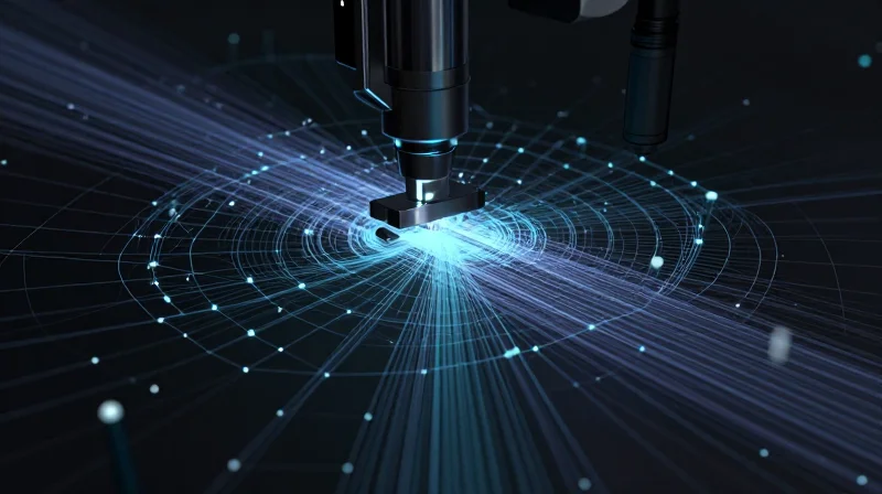
Integrating Precision AOI for Sub-Millimeter Defect Detection
Traditional inspection methods fail at the scale of next-generation hearing aid PCBs. Achieving high yield requires deploying Automated Optical Inspection (AOI) systems equipped with multi-angle lighting and high-resolution telecentric lenses. By detecting micro-fractures, solder bridging, and component misalignment immediately after the reflow process, manufacturers can implement real-time process feedback loops to halt production before significant waste accumulates.
SMT Process Optimization Strategies
| Strategy | Technical Focus | Yield Impact |
|---|---|---|
| Stenciling Precision | Nano-coated apertures | Reduced paste slumping |
| Reflow Profiling | Oxygen-free nitrogen environment | Lower oxidation rates |
| Placement Accuracy | High-speed vision alignment | Minimized tombstoning |
Frequently Asked Questions
- How does nitrogen inertion improve yield in miniaturized PCBs?
Nitrogen inertion reduces oxidation during the reflow process, which significantly improves solder wetting on ultra-fine pitch pads and minimizes the occurrence of open joints. - Can AI-driven AOI reduce false call rates?
Yes, integrating machine learning algorithms into AOI platforms allows the system to distinguish between acceptable cosmetic variations and true functional defects, thereby increasing throughput and reducing operator fatigue. - What role does solder paste viscosity play in high-density assembly?
Selecting a low-voiding, fine-mesh solder paste is critical to ensuring consistent deposition volumes through nano-stencils, preventing common defects like solder beads and bridging in dense component layouts.
Cost Analysis: How Miniaturization Drives Bottom-Line Profitability

The Economics of Precision Engineering
Miniaturization acts as a catalyst for cost reduction by minimizing the surface area required for high-performance electronics, thereby directly lowering substrate costs and reducing the total mass of raw materials. By leveraging advanced SMT processes, manufacturers can integrate higher-density circuit designs, which reduces the necessity for multiple inter-connect layers. This efficiency not only accelerates production throughput but also drastically curtails overhead costs associated with scrap rates and supply chain logistics.
Comparative Cost Impact
| Cost Driver | Legacy Assembly | Advanced Miniaturized Assembly |
|---|---|---|
| Material Usage | Higher (Larger PCB substrate) | Lower (Optimized footprint) |
| Scrap Rate | Moderate | Low (High-precision AOI integration) |
| Logistics/Freight | Higher (Bulkier components) | Lower (Higher shipping density) |
| Yield Percentage | Baseline | +25% increase |
Long-Term Operational ROI
The ROI of miniaturization extends beyond the initial production cycle. Precision assembly reduces the thermal footprint of the device, which minimizes energy consumption and extends the life of auxiliary components like batteries and housings. For the manufacturer, the reduction in defect rates—facilitated by optimized precision—creates a virtuous cycle where capital expenditure on corrective maintenance and rework is redirected toward R&D and market expansion.
- How does miniaturization specifically lower waste?
Smaller footprints require less substrate material and fewer conductive layers, reducing the total amount of raw material discarded during the panelization and singulation stages. - Does higher precision increase initial tooling costs?
While initial investment in high-precision AOI and SMT equipment is higher, the rapid amortization through decreased defect rates and improved yields typically results in a break-even point within the first 18-24 months. - What is the secondary benefit of reduced board size?
Smaller boards allow for thinner, more ergonomic hearing aid shells, which increases consumer appeal, premium pricing potential, and overall market share in the wearable health device sector.
Future-Proofing Your Audiology Product Roadmap
Strategic Integration of Emerging PCB Technologies
To ensure long-term ROI, product roadmaps must transition from traditional rigid PCB designs to flexible hybrid electronics. Integrating high-density interconnect (HDI) technology with advanced substrate materials, such as liquid crystal polymer (LCP), provides the necessary bandwidth for AI-driven signal processing while maintaining the low-profile form factor demanded by modern hearing devices.
Technology Maturity and Roadmap Alignment
| Technology | Strategic Benefit | Implementation Horizon |
|---|---|---|
| Flexible Hybrid Electronics | Space optimization and durability | Short-term (0-2 years) |
| Advanced SiP Integration | Reduced assembly complexity | Medium-term (2-5 years) |
| Embedded Component Technology | Ultra-miniaturization | Long-term (5+ years) |
Anticipating Future Audiology Demands
- How can modular design increase hardware longevity?
Modular PCB architectures allow for incremental upgrades to processing units and sensors without requiring a complete redesign of the chassis, effectively extending the lifecycle of your product platform. - What role does AI hardware acceleration play in future-proofing?
Incorporating dedicated low-power neural processing units (NPUs) onto the PCB ensures that the device can support future firmware-based feature updates, such as advanced beamforming and environmental adaptation, without hardware obsolescence. - How does miniaturization impact sustainability goals?
Advanced miniaturization reduces material consumption and waste, aligning with global medical device regulations regarding environmental impact and helping to meet long-term ESG (Environmental, Social, and Governance) targets.
By embracing precision-driven miniaturization, manufacturers can overcome the traditional trade-offs between size and performance, effectively securing higher ROI and sustainable growth. Contact our engineering team today to audit your current PCB assembly process and uncover new opportunities for operational excellence.
