
In the high-stakes world of medical imaging, signal clarity is non-negotiable. As ultrasound systems demand ever-increasing processing power within shrinking form factors, the burden shifts to the PCB designer. Mastering Design for Manufacturing (DFM) for high-layer HDI boards isn't just about functionality; it's about ensuring the long-term reliability of life-saving equipment.
The Challenge of High-Density Interconnects in Medical Imaging
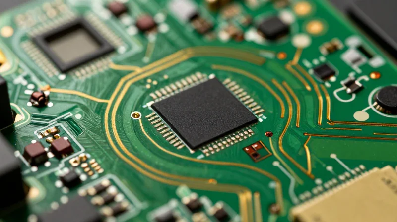
As ultrasound technology transitions from cart-based systems to portable and hand-held devices, the demand for High-Density Interconnect (HDI) PCBs has surged. Achieving miniaturization while maintaining signal integrity requires navigating extreme density constraints, where every micrometer of space impacts thermal dissipation, electromagnetic interference (EMI), and manufacturing yield.
Critical Engineering Constraints
Designing for high-layer HDI ultrasound boards necessitates a departure from standard PCB practices. The combination of dense component placement and high-speed data transmission channels introduces significant risk profiles regarding crosstalk and signal propagation.
| Design Factor | Primary Constraint | Manufacturing Impact |
|---|---|---|
| Trace Geometry | Impedance Control | Etch Factor Variations |
| Via Structure | Aspect Ratio | Plating Reliability |
| Thermal Density | Heat Dissipation | Material Tg Limits |
Common HDI Implementation Challenges
- How does layer count impact thermal management?
Increasing layers creates 'thermal pockets' where heat becomes trapped. Without strategic placement of thermal vias and high-Tg materials, the board may suffer from localized delamination or component degradation. - Why is signal integrity harder to maintain in HDI?
Reduced spacing between high-speed traces increases the likelihood of capacitive and inductive coupling, requiring rigorous simulation of crosstalk and differential pair skew. - What role does aspect ratio play in drilling?
High aspect ratios for microvias make uniform copper plating difficult. Poor plating leads to latent defects that may pass initial functional tests but fail under the thermal cycling inherent in medical environments.
Ultimately, the successful execution of HDI designs in ultrasound hardware requires an integrated approach to DFM (Design for Manufacturing). Engineers must balance the push for smaller footprints with the physical limitations of laser drilling, photo-imaging, and sequential lamination processes to ensure long-term clinical reliability.
Advanced Micro-Via Engineering and Drilling Precision
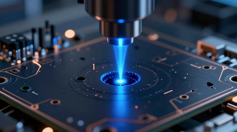
Laser Drilling Parameters and Precision Control
In high-layer HDI ultrasound boards, the transition to CO2 and UV laser hybrid systems is essential for achieving precise, tapered micro-via profiles. Successful drilling depends on balancing laser energy density, pulse frequency, and material composition. Over-ablation often leads to resin recession or damage to the underlying copper target pad, while insufficient energy results in incomplete via clearing (plugged vias). Engineers must characterize the specific laser-material interaction of high-frequency laminates, such as low-loss PTFE or reinforced epoxy systems, to maintain a consistent drill cycle.
The Role of Aspect Ratio in Via Reliability
The aspect ratio (AR)—the relationship between hole depth and diameter—is the primary constraint for reliable plating and thermal cycling survival. For high-layer counts, keeping the AR low is critical to allow electroplating chemistry to reach the base of the via.
| Parameter | Recommended Threshold | Impact of Violation |
|---|---|---|
| Max Aspect Ratio | 0.75:1 to 1:1 | Poor copper coverage, barrel cracks |
| Micro-via Diameter | 75µm - 100µm | Impedance mismatch, plating voids |
| Copper Target Pad | Via Diameter + 50µm | Drill breakout (annular ring issues) |
Advanced Micro-Via Engineering FAQs
- How does via-in-pad affect thermal performance?
Via-in-pad allows for shorter signal paths and better ground plane connectivity, which is vital for ultrasound sensitivity, but it requires precise solder mask plugging to prevent capillary wicking during assembly. - What is the primary cause of micro-via fatigue?
Thermal expansion mismatch between the copper plating and the dielectric material often leads to inner-layer separation or 'wedge voids' during board operation in high-heat medical environments. - Should laser drills be stacked or staggered?
Staggered vias are generally preferred for reliability as they distribute mechanical stress. However, stacked vias are often necessary for density; if stacking, ensuring planarization and reliable copper-filled interconnections is mandatory.
Optimizing Layer Stackups for Signal Integrity
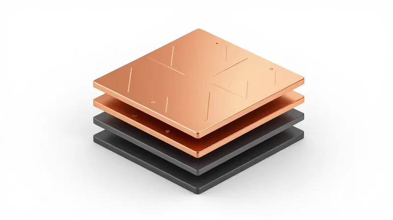
Strategic Layer Stackup Design for Ultrasound Integrity
In ultrasound imaging, signal integrity is paramount to maintaining high-resolution echo data. For high-layer HDI PCBs, the stackup must prioritize controlled impedance and return path continuity. A symmetric stackup is critical to preventing thermal warpage during the lamination process, which can lead to micro-via fracturing. Engineers should employ a 'signal-ground-signal' architecture where each high-speed signal layer is adjacent to a solid reference plane, ensuring a short, low-inductance return path.
| Constraint | Design Best Practice | Impact on Signal |
|---|---|---|
| Impedance Control | Maintain tight trace width tolerances (+/- 5%) | Reduces signal reflections |
| Crosstalk | Increase layer-to-layer spacing | Decreases inter-layer coupling |
| Return Path | Solid ground plane adjacency | Minimizes EMI and loop area |
| Symmetry | Balanced copper distribution | Prevents PCB board warping |
Mitigating Crosstalk in Densely Packed HDI Layouts
Ultrasound transducer arrays involve hundreds of sensitive traces. When traces are packed tightly in HDI structures, capacitive and inductive coupling often result in crosstalk. Use the '3W rule' for trace separation where possible, or utilize buried micro-vias to transition signals to internal layers, isolating them from adjacent noisy digital signals.
- How does stackup symmetry affect signal integrity?
Symmetry prevents thermal-mechanical stress during lamination, ensuring that micro-via registration remains precise and signal paths do not experience physical deformations that alter impedance. - Why prioritize ground plane proximity?
Adjacency to a solid reference plane minimizes the loop area for return currents, which is essential for containing electromagnetic interference in sensitive ultrasound circuitry. - What is the recommended approach for differential pairs?
Differential pairs must maintain strict coupling symmetry across the entire layer stack, utilizing consistent dielectric thickness to ensure phase matching and minimize skew.
High-Speed Signal Routing Best Practices
Differential Pair Routing and Impedance Control
Maintaining signal integrity in ultrasound front-end circuitry demands precise control over differential pair geometry. Because ultrasound systems process high-frequency signals from transducers, even minor deviations in trace width or spacing can cause significant phase mismatches and impedance discontinuities. Designers must prioritize length matching, typically held to within 5 mils for high-speed LVDS or JESD204C interfaces, to minimize skew and prevent common-mode noise conversion.
| Parameter | Design Rule for Ultrasound HDI | Reasoning |
|---|---|---|
| Intra-pair Skew | < 2 ps | Prevent EMI and signal degradation. |
| Reference Plane | Unbroken GND Plane | Maintain consistent return path. |
| Via Transitions | Back-drilling / Stitching | Minimize stub reflections. |
Crosstalk Mitigation and EMI Suppression
In high-density boards, the proximity of traces increases inductive and capacitive coupling, potentially corrupting sensitive receive-channel data. Implementing the 3H rule—where the distance between traces is three times the height from the reference plane—is essential. Furthermore, for ultrasound systems, aggressive use of ground stitching vias around high-speed buses acts as a shield, containing electromagnetic fields within the localized routing area.
Best Practices for HDI Routing FAQ
- How should high-speed traces transition between layers?
Utilize micro-vias with grounded reference plane transitions to minimize the length of the return path; avoid changing reference planes if possible to maintain impedance continuity. - Is serpentine routing recommended for length matching?
Use it sparingly. Serpentine delay lines should be kept wide and smooth to prevent impedance spikes at the turns, which can cause reflections at multi-gigabit speeds. - What impact does dielectric material have on routing?
Material consistency is paramount. Use low-loss, stable dielectric constants across the PCB to ensure predicted impedance models align with the final manufactured hardware.
Thermal Management and Material Selection
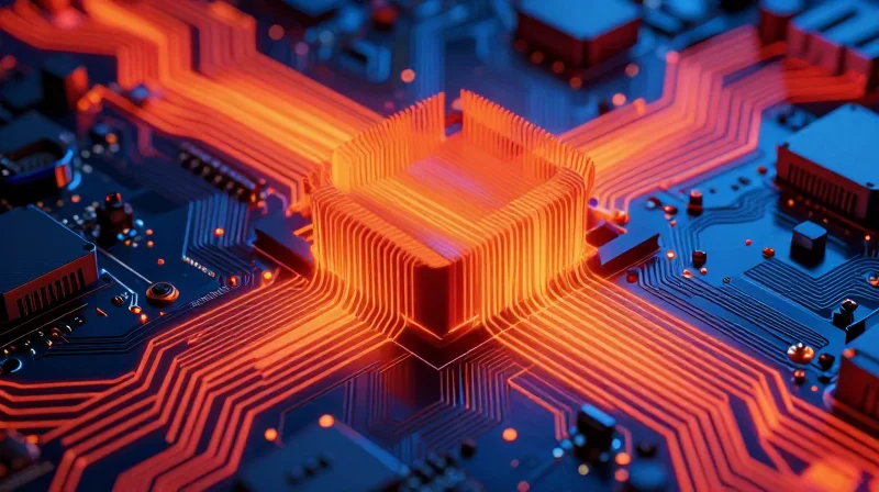
High-Tg Material Selection Strategies
Ultrasound systems generate concentrated heat during continuous signal processing cycles, necessitating the use of high-glass transition temperature (Tg) materials. Selecting a laminate with a Tg above 170°C and a low coefficient of thermal expansion (CTE) is non-negotiable for maintaining the Z-axis stability required for reliable micro-via integrity in HDI constructions.
| Material Property | Requirement for HDI Ultrasound | Benefit |
|---|---|---|
| Tg | > 170°C | Prevents substrate delamination |
| Td | > 340°C | Ensures thermal decomposition resistance |
| CTE(Z) | < 3.0% | Reduces micro-via barrel fatigue |
Thermal Relief and Copper Balancing
To prevent board warpage during the multi-lamination cycles inherent in high-layer HDI boards, designers must implement strict copper balancing. Asymmetric foil distribution leads to localized stress, which manifests as structural warping during the reflow process. Furthermore, thermal relief pads must be meticulously designed to prevent heat sinking issues during soldering while ensuring the thermal path is not bottlenecked.
- How does copper balancing affect HDI board reliability?
Uneven copper distribution causes internal stress during thermal excursions, leading to catastrophic warpage and potential failure of fine-pitch solder joints. - Why is CTE (Z-axis) critical for micro-vias?
As temperature increases, the board expands faster than the copper plating in the vias; low CTE materials keep these rates synchronized, preventing barrel cracking. - What is the role of thermally conductive adhesives?
In high-power ultrasound modules, thermal prepregs can bridge the gap between heat-generating components and internal ground planes, lowering overall junction temperatures.
Design Best Practices for Thermal Dissipation
1. Increase internal copper pours to act as heat spreaders.
2. Utilize staggered micro-vias to maintain solid thermal paths between layers.
3. Avoid large non-functional pads that impede thermal flow.
4. Distribute power-intensive components to prevent thermal hotspots.
DFM Rules for Laser Drill Alignment and Registration
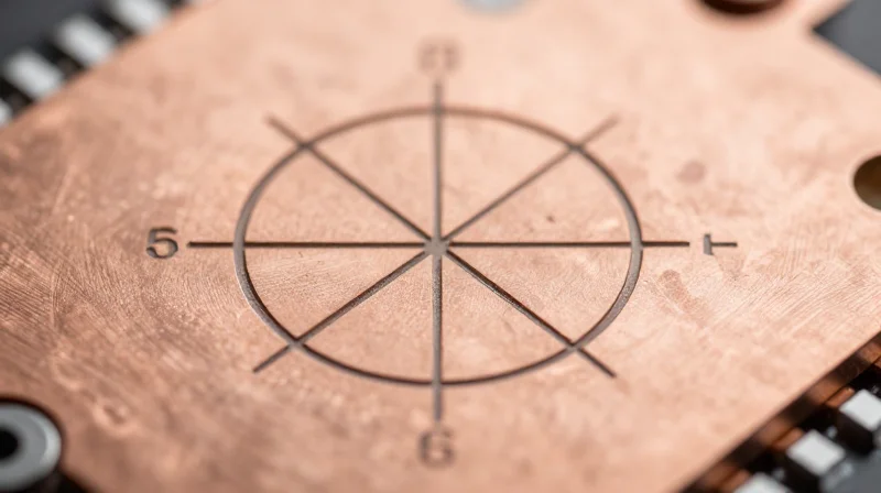
In the context of ultrasound imaging, where signal fidelity is paramount, even minor misalignments during laser drilling can result in open circuits or compromised impedance in microvias. Designers must account for the mechanical limitations of laser drilling systems by implementing generous pad-to-hole clearance ratios and strategically placing fiducials to accommodate material dimensional changes during the lamination process.
Key Design Rules for Laser Via Registration
- Annular Ring Requirements
Maintain a minimum target of 50µm for the capture pad to ensure that laser misregistration does not result in breakout, which can negatively impact high-frequency signal paths. - Drill-to-Copper Spacing
Apply a minimum clearance of 75µm between the laser-drilled via edge and internal copper features to prevent accidental shorts caused by registration drift during the drilling cycle. - Fiducial Design
Utilize local optical fiducials on every layer where laser drilling is initiated. Ensure these are etched with high-contrast finishes to allow machine vision systems to calculate precise drill offsets for each panel.
Registration Strategy Comparison
| Registration Technique | Best For | Tolerance Margin |
|---|---|---|
| Global Panel Fiducials | Standard HDI | +/- 50µm |
| Local Optical Fiducials | High-Layer Ultrasound PCBs | +/- 25µm |
| X-Ray Alignment | Complex Multi-Stackup | +/- 15µm |
Manufacturing Considerations for Material Stability
Ultrasound PCBs often utilize advanced high-Tg laminates that exhibit varying degrees of movement during lamination. To mitigate registration errors, designers should incorporate 'thieving' patterns in non-critical areas to balance copper distribution across the board surface, reducing the risk of local distortion that misleads laser drill alignment systems.
Reliability Testing: Validation for Medical Compliance
In the medical ultrasound sector, where diagnostic accuracy is paramount, HDI PCB reliability is non-negotiable. Reliability testing serves as the final gateway to clinical certification, verifying that complex high-density interconnections can withstand the rigors of medical environments without degradation. These protocols validate design robustness under stress, ensuring long-term field stability for life-critical imaging hardware.
Essential Reliability Testing Protocols
| Test Type | Primary Objective | Clinical Relevance |
|---|---|---|
| Cross-Section Analysis | Verification of hole wall quality and plating thickness. | Prevents internal interconnect failure in high-frequency transducers. |
| Thermal Shock (Cycling) | Evaluating fatigue resistance across CTE mismatches. | Ensures board integrity during rapid temperature changes in clinical settings. |
| Highly Accelerated Life Test (HALT) | Identifying hidden design flaws via vibration and temperature stress. | Predicts device longevity and critical failure points in portable scanners. |
Meeting Regulatory Compliance Standards
Medical compliance requires adherence to standards such as IPC-6012 (Class 3/3A) for rigid boards and IEC 60601 for medical electrical equipment. Testing must demonstrate that microvias and blind vias maintain electrical continuity under harsh operational conditions. Manufacturers must document every test iteration, providing a clear audit trail that links material batch numbers to specific performance results.
Frequently Asked Questions
- How does cross-sectioning impact HDI reliability?
It allows inspectors to measure the aspect ratio of microvias and verify the integrity of electroless copper deposition, ensuring no voiding exists within the high-density build-up layers. - Why is thermal shock testing critical for HDI PCBs?
Ultrasound devices experience internal heating during high-speed signal processing; thermal shock testing forces fatigue on solder joints and vias to simulate years of operation in minutes. - What is the role of IST (Interconnect Stress Testing)?
IST is used to monitor the resistance changes in the daisy-chain patterns of HDI boards, allowing for real-time detection of barrel cracking or laminate delamination under thermal loading.
Achieving reliability in medical ultrasound systems requires a holistic approach that bridges the gap between advanced design and precision manufacturing. By implementing these DFM strategies, engineering teams can reduce development cycles and ensure their systems meet the rigorous demands of clinical environments. Ready to optimize your next PCB project for high-performance imaging? Contact our engineering team today for a design audit.
