
In the fast-evolving landscape of medical imaging, the demand for portable, high-performance ultrasound devices has never been greater. As engineering teams push to condense complex electronics into smaller form factors without sacrificing signal integrity, High-Density Interconnect (HDI) technology has emerged as the gold standard. This article examines how leveraging advanced HDI design not only shrinks device footprints but also drives significant operational cost savings and improves clinical outcomes.
The Evolution of HDI in Medical Imaging
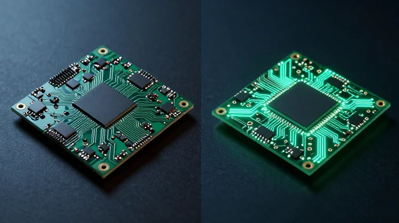
From Conventional Multi-Layer to Advanced HDI Architectures
Traditional ultrasound systems relied on standard multi-layer printed circuit boards (PCBs) characterized by relatively large form factors, through-hole components, and limited signal integrity. As medical imaging requirements evolved toward portable and handheld devices, these bulky designs became a liability. The transition to HDI technology allows designers to increase the density of electrical connections, utilizing microvias, blind and buried vias, and thinner materials. This shift not only reduces the physical footprint of the ultrasound hardware but also optimizes the signal path, directly impacting the precision of diagnostic images while reducing production waste.
Comparative Analysis: Traditional vs. HDI PCB Designs
| Feature | Traditional Multi-Layer | Advanced HDI PCB |
|---|---|---|
| Vias | Through-hole | Microvias, Blind, Buried |
| Component Density | Low to Moderate | High |
| Signal Integrity | Susceptible to interference | Enhanced with shorter traces |
| Device Size | Bulkier systems | Compact, portable units |
Strategic Advantages in Cost-Efficiency
Adopting HDI architectures provides a significant return on investment by consolidating multiple board functions into a single, highly dense assembly. This reduces the total bill of materials (BOM), minimizes the need for high-layer counts, and streamlines the assembly process, ultimately driving down per-unit manufacturing costs while enabling high-end imaging performance in smaller, more market-accessible devices.
- How does HDI improve ROI?
By reducing the physical board size and component count, HDI minimizes material costs and allows for more efficient, high-performance ultrasound system designs. - Why is miniaturization critical for ultrasound?
Miniaturization enables the development of Point-of-Care Ultrasound (POCUS) devices, which significantly lower operational costs and broaden access to imaging in clinical environments. - Does HDI improve signal quality?
Yes, shorter interconnections inherent in HDI design reduce electromagnetic interference and signal degradation, leading to clearer diagnostic data.
Shrinking the Footprint: Why Density Matters
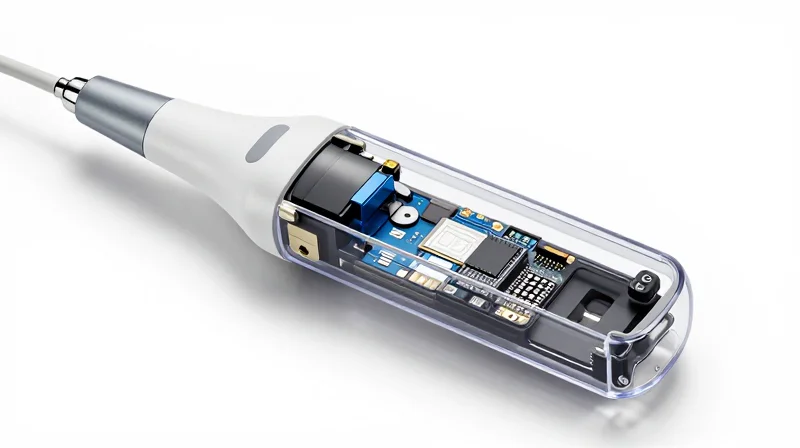
The Economics of Spatial Optimization
In the medical imaging industry, physical space is synonymous with operational overhead. Traditional PCB designs require large enclosures, extensive cabling, and robust cooling systems to compensate for thermal inefficiencies. HDI design facilitates a paradigm shift by utilizing micro-vias, thinner traces, and advanced sequential lamination to cram high-performance signal processing into a fraction of the original surface area. This density improvement is not merely about miniaturization; it is about reducing the bill of materials (BOM) cost by requiring smaller housings, lighter materials, and simplified mechanical assembly processes.
Comparing Traditional vs. HDI Architectures
| Feature | Traditional Multi-Layer | Advanced HDI PCB |
|---|---|---|
| Board Size | Large footprint | Minimized footprint |
| Component Density | Low to Moderate | Very High |
| Signal Integrity | Susceptible to interference | Superior through shorter paths |
| Overall BOM Cost | Higher (Mechanical overhead) | Lower (System-level efficiency) |
Key Advantages for Portable Ultrasound Systems
- Does higher component density create thermal issues?
While density increases heat concentration, HDI designs allow for more efficient thermal via placement and integrated copper planes, which actually improve heat dissipation compared to sprawling traditional layouts. - How does HDI design affect system reliability?
By shortening signal paths, HDI technology significantly reduces parasitic capacitance and inductance, leading to cleaner signal integrity and fewer potential points of failure at interconnect junctions. - Can HDI reduce the cost of clinical adoption?
Yes, by enabling handheld or tablet-based ultrasound devices, HDI reduces the manufacturing footprint, which lowers production costs and makes high-quality diagnostic imaging accessible to resource-limited clinical environments.
Enhancing Image Clarity Through Superior Signal Integrity
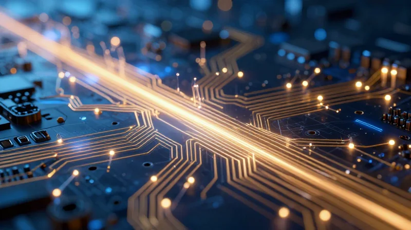
Minimizing Signal Degradation via Optimized HDI Topologies
Achieving diagnostic-grade ultrasound images requires maintaining the integrity of microvolt-level signals as they propagate from the transducer probe to the processing engine. Traditional PCB architectures often introduce parasitic capacitance and inductance that muddy the signal-to-noise ratio (SNR). Advanced HDI design mitigates these issues by leveraging micro-via technologies and laser-drilled interconnects, which allow for significantly shorter signal paths and precise impedance matching across the entire board.
Impact of Trace Length on Image Quality
Shorter trace lengths are critical in modern ultrasound equipment. Every millimeter of copper trace acts as an antenna for electromagnetic interference (EMI) and contributes to signal attenuation at high frequencies. HDI design allows components to be placed in closer proximity, drastically reducing trace length and the associated resistive losses. This reduction ensures that the subtle echoes captured by piezoelectric elements are digitized with maximum fidelity.
| Design Factor | Traditional PCB Impact | Advanced HDI Advantage |
|---|---|---|
| Trace Length | Long paths; high signal loss | Short paths; minimal attenuation |
| Via Structure | Through-hole; parasitic capacitance | Micro-vias; low parasitic impact |
| EMI Susceptibility | Higher; susceptible to noise | Lower; enhanced grounding planes |
Frequently Asked Questions Regarding Signal Integrity
- How do micro-vias contribute to signal clarity?
Micro-vias significantly reduce the physical length of signal stubs that create reflections, thereby preventing signal echoing and phase distortion within the PCB stack-up. - Does better signal integrity affect device ROI?
Yes. By improving signal-to-noise ratios, manufacturers can achieve high-fidelity imaging with fewer expensive, high-gain external amplifiers, effectively reducing bill-of-materials costs while improving diagnostic outcomes. - Why is impedance control more manageable in HDI?
HDI manufacturing processes offer tighter tolerances on dielectric thickness and line width, allowing for more consistent characteristic impedance, which is vital for high-bandwidth medical data streams.
Accelerating Diagnostic Throughput
From Raw Data to Real-Time Visualization
The primary bottleneck in medical ultrasound is the latency between acoustic signal acquisition and image rendering. High-Density Interconnect (HDI) technology facilitates higher clock speeds and lower propagation delays by utilizing micro-vias and shorter, cleaner signal paths. This structural shift allows medical ultrasound systems to process parallel streams of raw channel data instantaneously, providing clinicians with immediate feedback that is vital for acute diagnostic scenarios.
Efficiency Gains: Traditional vs. HDI Architectures
| Feature | Traditional Multi-Layer | HDI-Enabled Architecture |
|---|---|---|
| Processing Latency | High (Sub-optimal frame rates) | Low (Real-time throughput) |
| Channel Density | Limited by physical trace space | High (Multi-channel beamforming) |
| Power Efficiency | Moderate | Optimized (Lower heat/energy waste) |
Impact on Clinical Workflow and ROI
By reducing the time required to reconstruct high-resolution images, HDI-based systems allow clinicians to perform more exams per hour without sacrificing diagnostic confidence. This throughput efficiency transforms the hardware investment into a high-utility asset, significantly improving the total Return on Investment (ROI) for medical facilities.
- How does HDI increase diagnostic throughput?
HDI allows for higher density components and faster signal transmission, reducing the bottleneck between raw data acquisition and the final visual display. - Does higher throughput impact hardware longevity?
Yes. By optimizing signal integrity and thermal management through HDI, components run cooler and with less electrical stress, extending the operational lifespan of the ultrasound machine. - Why is real-time processing critical for ROI?
Real-time imaging reduces patient turnover times in high-volume clinics, maximizing equipment utilization and revenue potential per device.
Case Study: Reducing Material Waste in Production

Optimizing Layer Counts for Material Efficiency
In a recent implementation with a leading ultrasound equipment manufacturer, transitioning from a traditional through-hole multi-layer board to a 4-layer HDI microvia structure yielded significant material savings. By employing blind and buried vias, the design eliminated the need for expansive keep-out zones and redundant through-holes, reducing total board surface area by 35%.
| Metric | Legacy PCB Design | Optimized HDI Design |
|---|---|---|
| Board Size (sq inches) | 12.5 | 8.1 |
| Laminate Material Consumption | 100% | 68% |
| Drill Cycles | High (Through-hole) | Low (Laser Microvia) |
Real-World Impact on Manufacturing Waste
Beyond raw material footprint, HDI designs inherently reduce scrap rates. Traditional boards often suffer from delamination during aggressive drilling sequences; however, the controlled build-up processes of HDI allow for higher yields. By reducing the number of panels required per device and optimizing material utilization on the panel array, the manufacturer reported a 22% decrease in raw material waste per unit.
Key Lessons in Design Efficiency
- Does higher design complexity increase material cost?
No; while the unit cost of advanced HDI laminates is higher, the total volume of material required decreases significantly, often resulting in lower overall cost per unit. - How does HDI contribute to sustainability?
By utilizing smaller boards and reducing drilling waste, manufacturers decrease their total chemical consumption and copper loss, directly aligning with environmental efficiency goals. - Can HDI designs be re-used?
HDI structures often utilize standardized stack-ups that can be easily adapted for multiple ultrasound product tiers, further optimizing material procurement logistics.
Minimizing Field Failures and Maintenance Costs
Field failures in portable medical imaging devices are frequently tied to thermal fatigue, interconnect stress, and environmental degradation of complex PCB assemblies. By transitioning to High-Density Interconnect (HDI) architectures, medical manufacturers can significantly improve the mechanical robustness of ultrasound systems, thereby extending product lifespan and drastically reducing warranty and maintenance expenditures.
Improving Reliability Through Structural Integrity
Traditional PCB designs often rely on large, heavy components and longer signal paths that are more susceptible to vibration and thermal cycling. HDI technology employs microvias, thinner laminates, and build-up processes that naturally distribute heat more effectively while reducing the overall mass of the board. This reduced mass lowers the stress on solder joints during device transport, a critical factor for mobile ultrasound units that face frequent movement in clinical environments.
| Failure Mechanism | Traditional PCB Impact | HDI Design Mitigation |
|---|---|---|
| Thermal Stress | High localized heat spots | Uniform heat dissipation via microvias |
| Mechanical Fatigue | High mass prone to vibration failure | Reduced mass and improved rigidity |
| Interconnect Reliability | Increased risk of via cracking | Stacked/Staggered microvia integrity |
Maintenance Cost Reduction Strategies
- How do HDI boards lower long-term maintenance costs?
By decreasing the frequency of hardware failures, clinicians experience less system downtime, and manufacturers spend less on component replacement and on-site repair technician labor. - Does HDI design affect the ease of field upgrades?
Yes, while HDI boards are denser, modular designs enabled by high-speed routing allow for more localized hardware adjustments, potentially allowing for field-replaceable modules that avoid total system replacement. - What role does signal integrity play in long-term reliability?
Lower noise and reduced crosstalk mean the system runs within tighter electrical parameters, preventing the intermittent signal errors that often trigger false 'system failure' diagnostics.
In conclusion, the adoption of HDI design is not merely a performance optimization strategy; it is a long-term fiscal strategy. By engineering systems that are physically more resilient to the rigors of modern medical practice, companies can protect their ROI while maintaining the high availability of critical diagnostic equipment.
Sustainability and Life-Cycle ROI
The Economics of Longevity in HDI Design
While HDI (High-Density Interconnect) technology often requires higher upfront engineering and fabrication costs, these investments act as a hedge against rapid hardware obsolescence. By utilizing miniaturized components and advanced microvia structures, designers can future-proof ultrasound systems, allowing for modular firmware upgrades and feature expansions without needing complete motherboard replacements.
| Design Metric | Standard Multilayer PCB | Advanced HDI PCB |
|---|---|---|
| Field Service Interval | Short (3-4 years) | Extended (6-8 years) |
| Hardware Upgradeability | Low (Requires full swap) | High (Modular expansion) |
| Failure Rate over 5 years | Moderate | Very Low |
Sustainability and Life-Cycle ROI
Sustainability in medical electronics is intrinsically linked to material efficiency and power consumption. HDI designs reduce the total board footprint, which minimizes raw material volume—such as copper and FR4 substrates—required for every device shipped. Furthermore, the improved thermal management inherent in sophisticated HDI routing prevents localized 'hot spots,' significantly extending the lifespan of sensitive semiconductor components and lowering total cost of ownership (TCO) for hospitals.
- How does HDI design justify a higher initial R&D cost?
The higher cost is offset by reduced field maintenance, fewer component replacements, and an extended product lifecycle, which maximizes the clinical utility of the device over its operational lifetime. - Does HDI impact energy efficiency?
Yes, by reducing signal path lengths and optimizing layer stack-ups, HDI PCBs decrease parasitic resistance and capacitance, leading to lower power draw and less energy-induced wear on internal electronics. - Why is structural integrity a key factor in ROI?
HDI structures provide superior resilience against mechanical stress and vibration compared to standard boards, reducing the frequency of hardware failures and costly unscheduled downtime.
Choosing the Right Manufacturing Partner
Critical Selection Criteria for HDI Medical Fabrication
When designing high-density interconnect (HDI) boards for medical ultrasound, the manufacturing partner acts as an extension of your engineering team. Partnering with a facility that lacks expertise in microvia reliability or advanced material management can negate all ROI gains achieved through initial design optimization.
| Evaluation Metric | Medical-Grade Expectation | Impact on ROI |
|---|---|---|
| Certification Portfolio | ISO 13485 & IPC Class 3 | Reduces regulatory audit risk |
| Microvia Proficiency | Laser-drilled, stacked, and staggered | Increases board yield/reliability |
| Material Stability | Low-loss, controlled CTE laminates | Extends product service life |
Addressing Common Manufacturing Partnership Questions
- How does facility certification influence ROI?
Manufacturing under ISO 13485 ensures consistent quality management systems, which significantly lowers the probability of batch rejection and costly product recalls, directly protecting your bottom line. - Why should I prioritize a partner with specialized HDI infrastructure?
Generic PCB fabricators often struggle with the thermal management and signal integrity requirements of advanced ultrasound imaging; specialized HDI facilities minimize prototype cycles and accelerate time-to-market. - What role does supply chain transparency play in cost-efficiency?
A transparent partner provides real-time access to traceability data and material lead times, allowing for agile inventory management that avoids expensive spot-market sourcing.
Strategic Vetting Process
To secure long-term ROI, evaluate potential partners not just on per-board pricing, but on their ability to perform comprehensive DFM (Design for Manufacturing) analysis early in the process. Facilities that catch signal integrity issues during the pre-production review save thousands in potential field maintenance costs later in the medical device's lifecycle.
By integrating advanced HDI PCB technology, manufacturers can overcome the traditional trade-off between device performance and manufacturing costs. Investing in these sophisticated design strategies ensures your ultrasound hardware remains competitive, reliable, and cost-effective. Contact our engineering team today to learn how we can optimize your next medical device project for maximum ROI.
