
In the fast-paced security industry, the transition to high-resolution, AI-driven CCTV systems demands more from your mainboard than ever before. If your PCBA design isn't optimized for manufacturing, you risk costly delays and signal failures. This guide provides the blueprint for robust, scalable PCB design.
Understanding the Unique Challenges of Security Camera PCBs
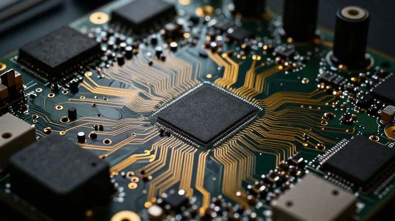
The Triad of Constraints: Space, Heat, and Data
Modern security camera mainboards are defined by a contradictory set of requirements: they must pack powerful image processing SoCs and high-resolution sensors into increasingly smaller enclosures while maintaining low-latency, high-bandwidth data transmission and effective heat dissipation. This tight integration forces engineers to push the limits of traditional Design for Manufacturing (DFM) rules.
| Constraint | Challenge | DFM Priority |
|---|---|---|
| Miniaturization | High component density in tight enclosures | Micro-via stack-up and pitch optimization |
| Thermal Management | SoC heat accumulation in restricted airflow | Thermal via arrays and copper balancing |
| Signal Integrity | EMI from high-speed CMOS sensors | Impedance control and stack-up symmetry |
Key Design Considerations for HDI Implementation
- Why are micro-vias critical for security camera boards?
Micro-vias are essential to connect high-density BGA packages found in advanced image processors, allowing for higher routing density without consuming precious surface real estate on outer layers. - How does signal speed impact board layout?
With the transition to 4K/8K resolution and high-frame-rate streaming, differential pair signals require strictly controlled impedance and minimal layer transitions to prevent signal attenuation and electromagnetic interference. - How can thermal bottlenecking be mitigated during design?
Engineers must employ strategic thermal relief patterns and dedicate internal copper planes as heat spreaders, effectively linking high-heat components directly to the board's structural ground or heat-sinking chassis.
Adhering to these principles requires a shift from traditional 'fit-and-forget' layout methods toward a holistic DFM approach. Designers must simulate thermal dissipation profiles early in the design cycle and ensure that the stack-up geometry supports both manufacturing yield and signal performance.
Strategic Layer Stack-up Design for EMI Shielding
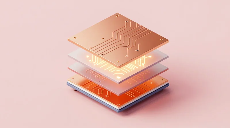
The Imperative of Reference Plane Continuity
In high-density interconnect (HDI) designs for security cameras, EMI is primarily governed by the integrity of the return current paths. A strategic stack-up must ensure that every high-speed signal layer is adjacent to a solid, unbroken reference plane. By maintaining a tight coupling between signal traces and return planes, you minimize the loop area—the fundamental mechanism for electromagnetic radiation.
Stack-up Strategy Guidelines
- Primary Grounding
Always prioritize a ground plane adjacent to signal layers to provide the lowest impedance path for return currents. - Avoid Plane Splitting
Splitting a ground plane under high-speed differential pairs forces return currents to take long, inductive paths, which creates significant EMI. - Layer Mirroring
Use symmetric stack-ups around the center to minimize thermal warping during the reflow process, which is critical for maintaining board flatness in thin camera modules.
Comparison of Common Stack-up Approaches
| Stack-up Type | EMI Shielding Efficiency | Best Use Case |
|---|---|---|
| 6-Layer Standard | Moderate | Low-cost, general-purpose surveillance sensors |
| 8-Layer HDI | High | 4K/8K AI-enabled camera processing modules |
| 10-Layer Blind/Buried | Excellent | Advanced multi-lens systems with complex routing |
Addressing Common EMI Concerns
- How do I mitigate edge radiation?
Use a '20-H' rule for power planes, ensuring they are pulled back from the edge of the ground plane to reduce fringing fields. - Does stack-up impact heat dissipation?
Yes; incorporate solid copper internal layers connected to thermal vias to draw heat away from the processor toward the camera chassis. - When should I use buried vias?
Use buried vias to free up surface routing space, allowing you to dedicate entire internal layers to reference planes without obstruction.
High-Speed Signal Integrity and Trace Routing
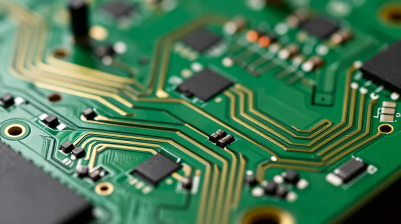
Advanced Impedance Control and Routing Strategies
For 4K video streams and neural processing, maintaining strict impedance control—typically 50Ω single-ended or 100Ω differential—is paramount to signal integrity. In HDI designs, where trace widths are sub-3 mil, manufacturing tolerances become the primary bottleneck. Designers must collaborate with PCB fabricators to define dielectric constants (Dk) that account for glass weave effects, which can introduce skew in high-speed differential pairs.
| Parameter | Design Rule | Mitigation Technique |
|---|---|---|
| Differential Pairs | 100Ω Nominal | Ensure tight coupling and equal length matching. |
| Trace Spacing | 3H Rule | Separate traces by 3x the dielectric height to reduce crosstalk. |
| Via Stubs | Back-drilling | Remove via stubs to prevent signal reflections. |
Crosstalk Mitigation in High-Density HDI
Crosstalk is exacerbated by the density of HDI boards, particularly near BGA components and high-speed SerDes interfaces. To minimize electromagnetic coupling, adopt strict orthogonal routing between adjacent signal layers and implement grounded coplanar waveguides where space permits. Avoiding long parallel runs and utilizing micro-vias instead of through-hole vias significantly reduces inductance and coupling loops.
Frequently Asked Questions
- How does glass weave impact signal integrity in security camera PCBs?
The heterogeneous nature of fiberglass and epoxy causes variations in propagation velocity. For high-speed lines, orienting traces at a slight angle to the weave or using spread-glass fabric styles minimizes intra-pair skew. - Is back-drilling mandatory for 4K video signal paths?
If the data rate exceeds 5Gbps, via stubs can act as antennas, causing resonant notches. Back-drilling is highly recommended to maintain signal bandwidth and integrity. - What role do reference planes play in HDI routing?
Reference planes must be unbroken directly under high-speed traces. Slotted planes or discontinuities force return currents to travel long paths, leading to increased emissions and crosstalk.
Optimizing Component Placement for Automated Assembly
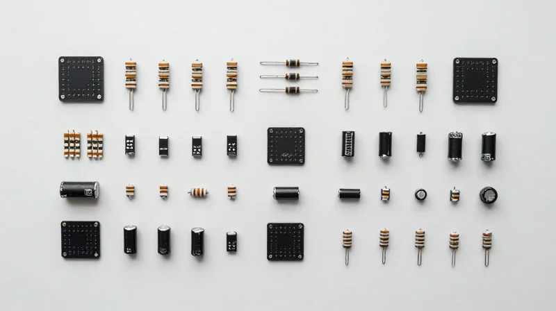
Strategic Component Placement for SMT Efficiency
In high-density interconnect (HDI) designs for security camera mainboards, component placement is the primary driver of SMT throughput. By adhering to a standardized grid-based placement strategy, designers minimize nozzle travel time and enable high-speed pick-and-place operation, directly reducing manufacturing costs and rework rates.
Orientation and Grid Standards
Consistency in component orientation is non-negotiable for large-scale production. All passive components, such as decoupling capacitors and resistors supporting the camera's image sensor, should follow a uniform orientation to streamline vision system processing. Designers should utilize a fine-pitch grid (e.g., 0.5mm or 0.25mm) to ensure CAD tools maintain precise alignment during the routing phase.
| Placement Metric | Best Practice | Manufacturing Benefit |
|---|---|---|
| Orientation | Uniform (0° or 90°) | Reduced vision system cycle time |
| Grid Alignment | Snap-to-grid (0.5mm) | Improved SMT machine throughput |
| Component Spacing | Min 0.2mm edge-to-edge | Prevents bridging and enables rework |
DFM Considerations for Rework and Inspection
- How does component density impact AOI?
Extreme density can create 'shadowing' effects where taller components block the line of sight for Automated Optical Inspection (AOI) cameras, necessitating strategic placement of low-profile components near sensors. - What is the primary constraint for rework?
Thermal relief and minimum clearance buffers around BGA packages are critical; without sufficient space, traditional soldering irons or hot-air rework stations cannot access target pins without damaging adjacent components. - Should fine-pitch parts be placed on both sides?
Avoid placing heavy or high-pin-count components on the bottom side if possible; if necessary, ensure they are placed such that they do not require secondary wave soldering, which risks bridge formation.
/* Design Rule Check (DRC) Guideline Example */
const min_component_spacing = 0.25; // mm
const orientation_tolerance = 0;   // Degrees

function validatePlacement(component) {
  if (component.spacing < min_component_spacing) return false;
  return true;
}
Thermal Management Solutions for High-Density Boards
Integrated Thermal Strategies for HDI Boards
High-density interconnect (HDI) boards, particularly those driving AI-based video analytics in security cameras, create significant localized heat flux. To prevent thermal throttling, designers must prioritize heat dissipation pathing during the initial layout phase, treating thermal management as a critical signal integrity requirement rather than an afterthought.
Thermal Via Arrays and Heat Sinking
Thermal vias serve as the primary conduit between active heat-generating components—such as SoC (System on Chip) processors and power management ICs—and the internal ground planes. Implementing a high-density matrix of copper-filled vias directly under the thermal pad is mandatory to minimize thermal resistance. For ultra-compact designs, consider using microvias to reduce the inductive loop area while maximizing heat transfer efficiency.
| Thermal Strategy | Implementation Priority | Performance Impact |
|---|---|---|
| Copper-Filled Via Matrix | High | Maximized heat sinking to internal planes |
| Thermal Interface Material (TIM) | Medium | Essential for coupling to chassis |
| Split Power Planes | Low | Prevents localized hotspots in dense zones |
Component Distribution and Airflow Optimization
In a confined CCTV chassis, component placement directly influences internal airflow dynamics. Avoid clustering high-power components in a single quadrant. Instead, utilize a 'distributed thermal load' strategy where power-hungry devices are spaced to prevent overlapping thermal envelopes. Furthermore, ensure that high-profile components do not obstruct potential convective airflow paths.
- How do thermal vias impact signal integrity?
While essential for cooling, dense via arrays can create discontinuities in ground planes; ensure these vias do not obstruct high-speed differential pair return paths. - Is heat sinking to the chassis effective in plastic enclosures?
In non-metallic enclosures, rely on internal heatsinks coupled to a metallic internal structural frame or thermal piping to transport heat away from the board surface. - What is the role of copper weight in thermal management?
Increasing internal copper weight (e.g., from 0.5oz to 1oz) significantly improves the lateral thermal conductivity of the board, allowing for better heat spreading across the entire PCB surface.
Solder Mask and Silkscreen Best Practices
Solder Mask Registration and Clearance
For HDI boards, solder mask registration must be strictly controlled to prevent accidental exposure of copper traces or impedance-controlled signals. A minimum registration tolerance of 2 mils (0.05mm) is recommended for high-density areas to accommodate board expansion and drilling registration shifts. Use solder mask defined (SMD) pads for BGA components to improve solder joint reliability, while ensuring non-solder mask defined (NSMD) pads are reserved for components requiring mechanical stress relief.
| Parameter | Recommended Value | Design Rationale |
|---|---|---|
| Mask Registration Tolerance | 2.0 mil (0.05mm) | Prevents solder bridge and shorts |
| Web Between Pads | 3.0 mil (0.076mm) | Ensures effective mask adhesion |
| Solder Mask Clearance | 2.0 - 4.0 mil | Standard pad-to-mask offset |
Silkscreen Standards for Precision Assembly
Clear labeling is essential for high-density boards, especially given the compact nature of camera modules. Avoid placing silkscreen text over solder pads or vias, as ink contamination can impede solder wetting. Implement a professional nomenclature system that includes polarity indicators and pin-one markings that remain visible after components are mounted.
- How do I ensure visibility on dense boards?
Utilize a minimum line width of 6 mil and a text height of 30 mil; for extremely dense areas, use high-contrast ink or laser marking to maintain legibility without violating clearance rules. - Should silkscreen cover test points?
Never place silkscreen over test pads or probe points; this prevents physical contact with automated test equipment and can cause failure during functional verification. - Is clipping allowed?
Implement automatic clipping to ensure the silkscreen layer is automatically truncated whenever it overlaps with solder mask or component pads, preventing manufacturing defects.
Manufacturing Best Practices
# Example constraint configuration for PCB CAD software
CONSTRAINT_SOLDER_MASK_REGISTRATION = 0.05mm
CONSTRAINT_SILK_TO_PAD_CLEARANCE = 0.15mm
MIN_TEXT_WIDTH = 0.15mm
Standardizing Design Reviews and DFM Verification
The Necessity of Automated DFM Verification
In the context of high-density interconnect (HDI) boards for security hardware, manual inspection is prone to human error and cannot keep pace with the complex design iterations required. Automated DFM (Design for Manufacturing) verification tools serve as the first line of defense by identifying critical violations—such as insufficient annular rings, trace-to-via clearance errors, or improper solder mask opening ratios—early in the design cycle when changes are least expensive to implement.
Cross-Functional Review Protocols
Standardization hinges on structured cross-functional reviews. By integrating electrical, thermal, and manufacturing engineers into a unified sign-off process, the team can address conflicts between performance requirements and physical fabrication constraints before a design is finalized for mass production.
| Review Stage | Key Focus Area | Objective |
|---|---|---|
| Pre-Layout | Stackup and Material | Optimize layer count and thermal performance. |
| Mid-Layout | Routing and Clearance | Verify HDI density and signal integrity constraints. |
| Post-Layout | DFM/DFA Audit | Final check against assembly and solder requirements. |
Common DFM Verification Queries
- Why is automated checking superior to manual review?
Automated checks provide comprehensive coverage across millions of net combinations, whereas manual reviews often miss isolated violations in dense multi-layer boards. - How does DFM standardization affect camera unit cost?
Standardized reviews reduce the frequency of board revisions and field failures, which directly lowers the total cost of ownership through higher initial assembly yields. - What is the most critical check for HDI boards?
Ensuring the via-in-pad and micro-via alignment is accurate to avoid plating voids and interfacial failure during the reflow process.
Mastering these DFM protocols transforms your design process, ensuring your hardware is as reliable as the security footage it captures. Ready to optimize your next production run? Contact our engineering team today to audit your design files and eliminate costly manufacturing bottlenecks.
