From the smartphones in our pockets to the complex machinery of industrial automation, MOSFET transistors are the unsung heroes quietly enabling the digital revolution. These tiny powerhouses, ubiquitous in modern electronics, control the flow of electricity with remarkable efficiency and precision. This article delves into the intricacies of MOSFET transistors, shedding light on their working principles, types, and diverse applications, providing a thorough understanding of these foundational semiconductor devices.
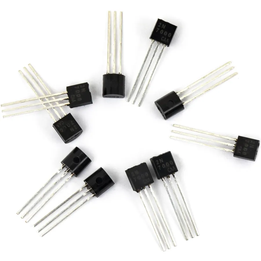
Metal-Oxide-Semiconductor Field-Effect Transistors (MOSFETs) are fundamental components in modern electronics, acting as voltage-controlled switches or amplifiers. As a type of Field-Effect Transistor (FET), their operation is based on modulating the conductivity of a channel via an applied electric field, providing superior control and efficiency in a wide range of applications.
The basic structure of a MOSFET includes four key terminals: the source (where charge carriers enter), the drain (where charge carriers exit), the gate (which controls the channel conductivity), and the substrate (the underlying semiconductor material). Understanding these components is essential for comprehending how MOSFETs function as the workhorse of semiconductor technology.
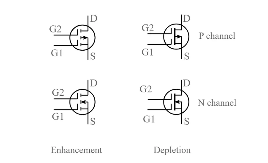
MOSFET transistors are broadly classified into two primary types: N-channel (NMOS) and P-channel (PMOS). These classifications are based on the type of charge carriers that enable current flow through the channel, fundamentally impacting their operational characteristics and applications in circuit design.
| Feature | N-Channel (NMOS) | P-Channel (PMOS) |
|---|---|---|
| Majority Charge Carriers | Electrons | Holes |
| Channel Formation | Inversion of a p-type substrate | Inversion of an n-type substrate |
| Gate Voltage for Conduction (Enhancement Mode) | Positive voltage relative to source | Negative voltage relative to source |
| Gate Voltage for Conduction (Depletion Mode) | Zero or negative voltage relative to source | Zero or positive voltage relative to source |
| Typical Applications | Low-side switching, logic gates, high-speed circuits | High-side switching, power management, analog circuits |
| On-State Resistance | Generally lower for same size device | Generally higher for same size device |
| Switching Speed | Faster switching speed due to higher electron mobility | Slower switching speed due to lower hole mobility |
The choice between NMOS and PMOS depends heavily on the application. NMOS transistors, with their higher electron mobility, are generally preferred in digital logic for their faster switching capabilities. Conversely, PMOS transistors are often used in high-side switching or when a lower on-resistance is required at a negative gate voltage. Complex integrated circuits leverage both types in complementary configurations (CMOS), which offer high noise immunity and low power consumption.
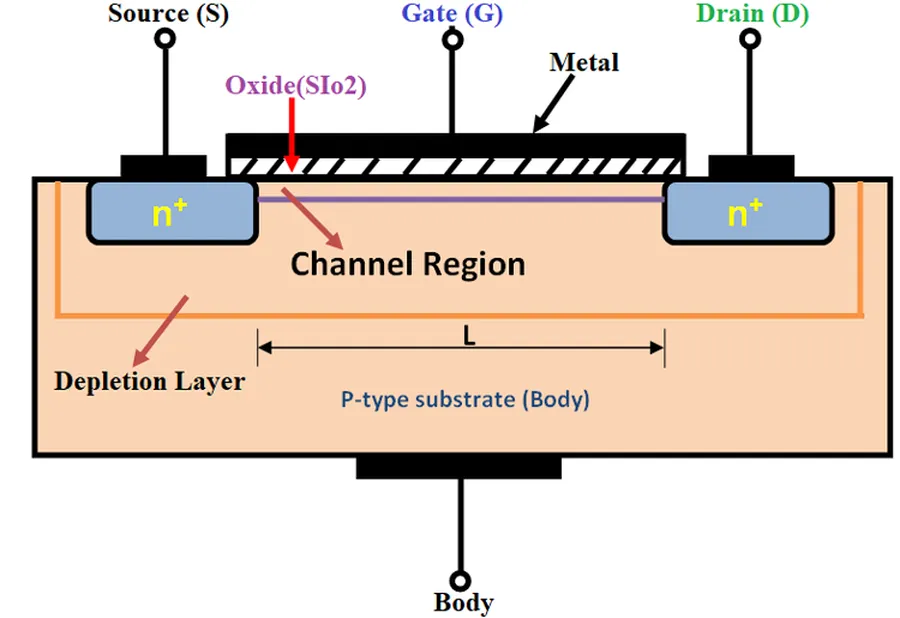
The operation of a Metal-Oxide-Semiconductor Field-Effect Transistor (MOSFET) hinges on the principle of controlling the conductivity of a channel between the source and drain terminals by applying a voltage to the gate terminal. This control mechanism allows MOSFETs to function as electronic switches or amplifiers in a wide variety of applications.
At its core, a MOSFET's functionality is based on the modulation of a conductive channel via an electric field. This channel, located between the source and drain, is initially non-conductive in its resting state. The application of a voltage to the gate terminal creates an electric field that either enhances or depletes the charge carriers in the channel, depending on the MOSFET's type (N-channel or P-channel).
In an N-channel MOSFET (NMOS), applying a positive voltage to the gate attracts electrons to the channel region, creating a conductive pathway and allowing current to flow from the drain to the source. Conversely, in a P-channel MOSFET (PMOS), applying a negative gate voltage attracts holes to the channel, also facilitating current flow. The gate is electrically insulated from the channel by a thin layer of silicon dioxide (SiO2) hence the name Metal-Oxide-Semiconductor. This insulation enables the gate to control channel conductivity with minimal current flow into the gate terminal. This makes MOSFET an extremely efficient device for switching and amplification purposes.
MOSFET transistors exhibit three primary operating regions: Cutoff, Triode (also known as Linear), and Saturation. Understanding these regions is crucial for designing circuits as they dictate the transistor's behavior and suitability for specific applications. Each region is defined by the relationship between the gate-source voltage (VGS) and the drain-source voltage (VDS), and they result in significantly different current flow characteristics.
| Operating Region | VGS Condition | VDS Condition | Drain Current (ID) Behavior | Application Examples |
|---|---|---|---|---|
| Cutoff Region | VGS < Vth (Threshold Voltage) | Any VDS | ID ≈ 0 (Ideally zero, minimal leakage current) | Switch in OFF state; Logic circuits where the transistor should not conduct |
| Triode/Linear Region | VGS > Vth | VDS < VGS - Vth | ID increases almost linearly with VDS. The MOSFET acts like a variable resistor. | Small-signal amplifiers, Variable resistors, Analog switches (when a small VDS is needed). |
| Saturation Region | VGS > Vth | VDS > VGS - Vth | ID is relatively constant and primarily depends on VGS, and relatively independent of VDS | Amplifiers, high speed switching applications, current sources. |
In the **Cutoff Region**, the MOSFET is essentially off, and very little current flows between the drain and source. This region is essential when the MOSFET is being used as a switch in an 'off' state. The MOSFET enters this region when the gate-source voltage is below the threshold voltage (Vth).
The **Triode or Linear Region** is characterized by the MOSFET acting like a voltage-controlled resistor. Here, the drain current increases almost linearly with the drain-source voltage (VDS), and the MOSFET's resistance can be modulated through the gate voltage. It occurs when the gate-source voltage (VGS) is greater than the threshold voltage (Vth), and when VDS is less than VGS-Vth. This mode is useful for low-voltage applications and analog circuits.
In the **Saturation Region**, the drain current becomes relatively constant and largely independent of VDS, it is primarily controlled by VGS. This occurs when VDS is greater than or equal to VGS-Vth. This is essential for amplifier circuits, where a constant current output is needed based on the gate input, and also for high-speed switching.
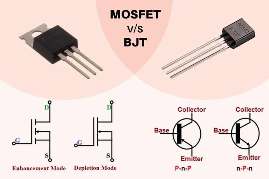
MOSFETs (Metal-Oxide-Semiconductor Field-Effect Transistors) and BJTs (Bipolar Junction Transistors) are fundamental semiconductor devices, but they differ significantly in their structure, operation, and performance characteristics. This section will highlight these key differences, focusing on the advantages of MOSFETs, particularly in modern electronic applications.
| Feature | MOSFET | BJT |
|---|---|---|
| Control Mechanism | Voltage-controlled (gate voltage) | Current-controlled (base current) |
| Input Impedance | Very High | Relatively Low |
| Power Consumption | Lower (minimal gate current) | Higher (base current required) |
| Switching Speed | Generally Faster | Slower for high-frequency applications |
| Temperature Stability | Generally good temperature stability | More susceptible to temperature changes |
| Operating Region | Cutoff, Triode/Linear, Saturation | Cutoff, Active, Saturation |
| Majority Carrier | Unipolar device (electrons or holes) | Bipolar device (both electrons and holes) |
| Structure | Gate, Source, Drain, Insulating Layer | Base, Collector, Emitter |
The voltage-controlled nature of MOSFETs offers several advantages. Their extremely high input impedance means they draw very little current from the driving circuit, leading to lower power consumption and simplified circuit design. This is a marked contrast to BJTs, which require a continuous base current, resulting in a lower input impedance and higher power dissipation. Furthermore, MOSFETs generally exhibit faster switching speeds than BJTs, making them better suited for high-frequency applications such as in modern digital electronics and power supplies. Though BJTs can offer higher current gain in some applications, MOSFETs superior characteristics, especially their low power consumption and high-speed switching make them the preferred choice for many modern applications.
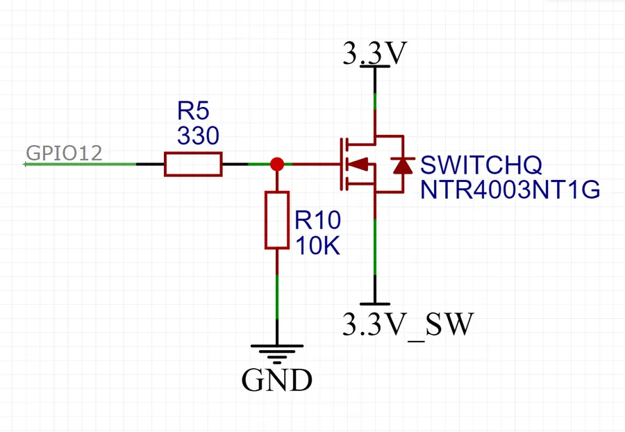
MOSFETs (Metal-Oxide-Semiconductor Field-Effect Transistors) are indispensable components in modern electronics, serving a diverse range of functions from high-speed switching to signal amplification. Their versatility stems from their ability to control current flow with minimal power consumption, making them ideal for a wide array of applications.
The versatility of MOSFETs enables a wide range of electronic devices. They are integral to almost all modern electronics, demonstrating their significance and continued importance in shaping technology.
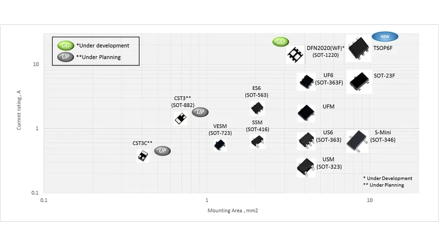
Selecting the appropriate MOSFET for a given application requires a thorough understanding of both the available packaging options and the critical electrical parameters. This guide provides a practical overview to navigate these considerations.
| Package Type | Description | Typical Applications | Pros | Cons |
|---|---|---|---|---|
| TO-220 | Through-hole package with a single mounting tab. Common for moderate power applications. | Power supplies, motor control circuits, audio amplifiers | Easy to mount and heatsink, widely available | Bulkier than surface mount, limited pin count |
| TO-247 | Larger through-hole package, similar to TO-220 but with a larger tab for better heat dissipation. | High power inverters, high current power supplies | Improved heat dissipation compared to TO-220 | Larger footprint, higher cost than TO-220 |
| D2PAK (TO-263) | Surface-mount package with gull-wing leads. Suitable for moderate to high power. | Switching power supplies, automotive electronics | Surface mount, compact, good thermal performance | Requires surface mount soldering, more complex assembly |
| DPAK (TO-252) | Smaller surface-mount package than D2PAK, good for moderate power applications. | DC-DC converters, power management | Compact surface mount, good thermal performance | May require specialized heat sinking, limited power rating |
| SOT-23 | Very small surface-mount package, for low-power applications. | Portable devices, signal processing circuits | Extremely compact and space saving | Limited power handling, requires specialized pick-and-place |
When selecting a MOSFET, consider these key parameters:
The appropriate selection should also be based on specific application needs. For example, high-frequency switching applications will demand fast switching speeds and low gate charge, whereas high-power applications require robust current and thermal handling capabilities. Careful datasheet review is essential to ensure a component's parameters meet the demands of its intended environment.
This section addresses common queries about MOSFET transistors, providing clear and concise answers to enhance understanding of their function, types, and applications. We aim to clarify the key differences between MOSFETs and other transistor types, and provide insights into their appropriate use cases.
The field of MOSFET technology is continuously evolving, driven by the demand for higher performance, increased energy efficiency, and more compact electronic devices. Emerging trends encompass novel materials, advanced fabrication techniques, and innovative applications, all aimed at pushing the boundaries of what's achievable with these ubiquitous transistors.
In conclusion, MOSFET transistors are fundamental building blocks of modern electronics, offering efficient control over electrical currents in a myriad of applications. Their unique properties, including the ability to switch quickly and efficiently with minimal power consumption, have made them indispensable in everything from computers to power supplies. As technology continues to advance, MOSFETs will undoubtedly continue to play a pivotal role in shaping the future of electronic devices. Understanding their functionality and capabilities is key for anyone involved in electrical engineering and beyond, paving the way for innovations in transistor-based technology.

