In today's rapidly evolving tech landscape, Printed Circuit Boards (PCBs) are the unsung heroes powering our devices. From smartphones to sophisticated medical equipment, PCBs form the crucial foundation. This article dives deep into the world of PCB printing, exploring different methods, key considerations, and how you can leverage this technology for your prototyping and production needs. Whether you're an engineer, a hobbyist, or an entrepreneur, understanding PCB printing is crucial in bringing your ideas to life. We'll bridge the gap between complex electronics and practical application, shedding light on this essential component of modern innovation.
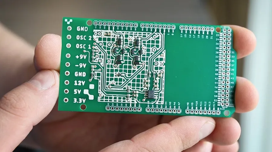
PCB printing, at its core, is the process of transferring a designed circuit pattern onto a non-conductive substrate, typically a fiberglass composite, using specialized techniques. This is the fundamental step in creating a printed circuit board (PCB), which serves as the backbone of most electronic devices. The process involves accurately applying conductive materials, usually copper, to the board in specific patterns to facilitate electrical connections between components.
The key elements involved are the substrate material, the conductive material and the method used to transfer the circuit design. The accuracy of this transfer is essential to the functioning of the finished product. Below is a breakdown of these key components:
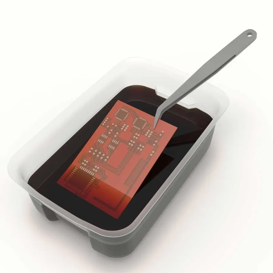
The fabrication of printed circuit boards (PCBs) relies on several distinct printing methodologies, each offering a unique balance of cost, precision, and applicability. Understanding these methods is crucial for selecting the most appropriate technique for a given project, be it a simple prototype or a complex mass-produced electronic device. This section will explore traditional etching, laser direct imaging (LDI), and inkjet printing, outlining the advantages and disadvantages of each.
| Method | Description | Pros | Cons | Typical Applications |
|---|---|---|---|---|
| Traditional Etching | A subtractive process where unwanted copper is removed using chemical etchants. | Low cost for simple designs, suitable for bulk production. | Lower precision, chemical waste, limited design complexity. | Basic single or double-layer PCBs, through-hole components. |
| Laser Direct Imaging (LDI) | A maskless process using a laser to directly pattern the photoresist layer. | Higher precision than traditional etching, allows for finer features, faster prototyping. | Higher initial equipment cost, can be slower for large volume production. | High-density PCBs, fine-pitch components, multi-layer boards. |
| Inkjet Printing | A digital printing process that deposits conductive inks directly onto the substrate. | Maskless and additive, flexible design, lower material usage, supports rapid prototyping. | Higher material cost, potential issues with ink uniformity, limited conductive material options | Flexible PCBs, printed electronics, rapid prototyping with custom layouts. |
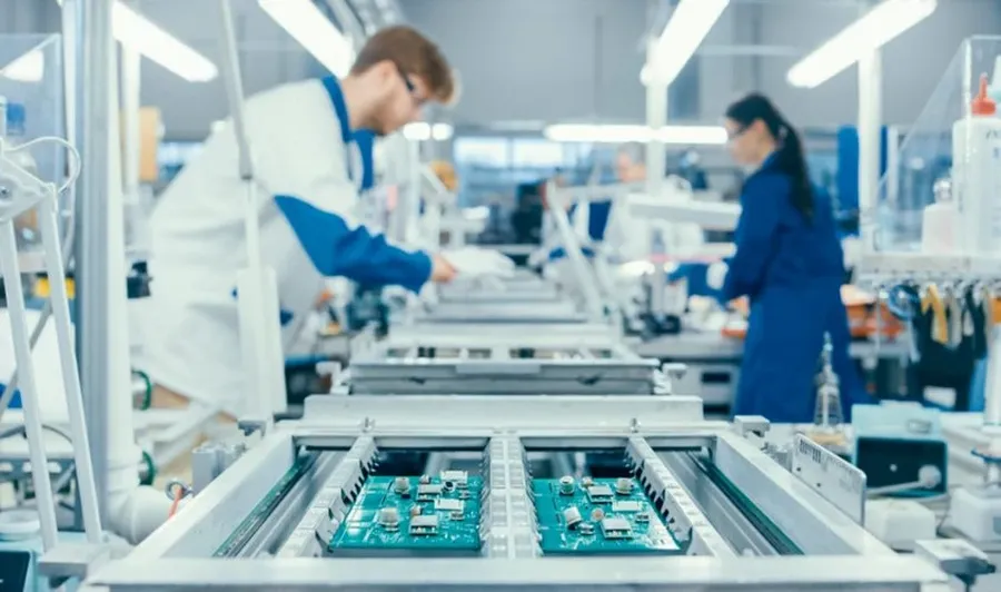
Selecting the appropriate PCB printing service is crucial for the success of any electronics project. This decision involves evaluating various factors such as cost, turnaround time, material quality, and certifications, as well as determining whether to use an online service or a local manufacturer. A thorough understanding of these elements will ensure that the chosen service aligns with the project's specific requirements and budget.
| Factor | Online PCB Printing Services | Local PCB Manufacturers |
|---|---|---|
| Cost | Often lower for standard designs and quantities due to economies of scale. | May be higher for small runs or custom requirements, but potentially more competitive for large orders. |
| Turnaround Time | Can vary widely; expedited options are available but can incur additional cost, average lead times need to be considered for overseas manufacturing. | Potentially faster for simple designs and local services, and could be easier to have a better communication channel with the service team. |
| Material Quality | Usually offer a range of materials with specifications, but quality control can be variable, the choice of materials may be limited. | May provide more flexibility in material selection, and higher assurance of quality, with in-house quality check control. |
| Certifications | Certifications are usually displayed on the website, but verifications can be hard to obtain if needed for compliance. | More likely to be compliant with specific industry standards, and easier to verify. |
| Communication | Communication is often asynchronous and can be less direct. | Direct communication with engineers and quick feedback is possible. |
| Minimum Order Quantity (MOQ) | May have lower minimum order requirements, which suits prototypes or small runs. | May have higher minimum order requirements which is more suited for mass production. |
| Complexity | Best suited for standard designs, but some offer advanced capabilities. | May offer greater flexibility for complex designs, custom requirements and tighter specifications. |
Understanding the pricing structure of PCB printing is crucial for managing project budgets effectively. The cost is influenced by a combination of factors including the quantity of boards, the complexity of the design, the materials used, and the required turnaround time. Optimizing these elements can lead to significant cost savings without compromising quality.
| Cost Factor | Impact on Cost | Optimization Strategies |
|---|---|---|
| Quantity | Higher volumes typically reduce the per-unit cost due to economies of scale. | Consolidate multiple prototypes or projects into a single order; consider batch production for larger needs. |
| Complexity | Factors such as layer count, via type, and trace width increase complexity and, therefore, cost. | Simplify designs when possible; minimize layer count and use standard via sizes; follow DFM (Design for Manufacturability) guidelines. |
| Materials | Different materials (e.g., FR-4, Aluminum, Rogers) vary significantly in price, impacting total cost. | Choose the most cost-effective materials that meet the required performance specifications. |
| Turnaround Time | Rush production with shorter lead times incurs higher costs. | Plan projects well in advance; select standard turnarounds when possible to avoid rush fees. |
| Surface Finish | Different surface finishes, such as ENIG, HASL, or OSP, have varied costs. | Select the most cost-effective finish that meets the application requirements; choose standard finishes over specialized ones when practical. |
| Board Size | Larger boards require more material and more processing time, driving up costs. | Optimize the board size to fit the components closely; panelize designs to maximize the manufacturer's material use. |
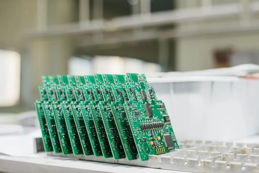
PCB printing plays a pivotal role in rapid prototyping, enabling engineers to quickly transform designs into physical prototypes for testing and validation. This section delves into the intricacies of how PCB printing facilitates quick turnarounds, focusing on the essential aspects that designers and engineers should consider for efficient prototype development.
The ability to rapidly iterate is paramount in the prototyping phase. Selecting a PCB printing service that offers fast turnaround times is crucial to minimize development cycles. These services often employ streamlined processes and prioritize quick-turn orders, allowing for quicker design revisions and validation. Here's a look at the key factors to prioritize:
In addition to choosing the right printing service and optimizing design, a clear understanding of potential design errors is crucial to avoid additional turnaround time. The following table provides the possible issues and solutions for the prototyping of PCB.
| Issue | Description | Solution |
|---|---|---|
| Insufficient Trace Width | Traces that are too narrow can cause signal integrity problems or lead to open circuits due to excessive resistance. It could also lead to over etching. | Adhere to manufacturer recommended minimum trace widths based on the current carrying requirements. |
| Insufficient Spacing Between Conductors | Inadequate spacing between traces, pads, and other conductive elements can lead to short circuits. | Ensure adequate spacing is maintained based on the voltage, material, and other requirements. |
| Incorrect Via Design | Poorly designed vias can cause signal impedance issues. This includes improper drill sizing or pad size. | Use appropriate via sizes based on manufacturing parameters and impedance requirements. |
| Poor Solder Pad Design | Incorrect solder pad dimensions can lead to issues during assembly. Too large of a pad and it could lead to solder bridging or cold joints, and too small could lead to lifting. | Design pads using the recommended component land pattern dimensions and solder specifications. |
| Missing Fiducials | Without proper fiducials, automated assembly processes can be hampered, leading to inaccuracies. | Include fiducials on your board using the correct size, shape, and clearances, to ensure proper alignment |
| Incorrect Layer Stacking | Incorrect layer stack configuration can cause signal issues. Poor stack up may also lead to manufacturability issues or higher impedance than expected. | Adhere to manufacturer specifications and conduct impedance calculations for the correct layer stack up. |
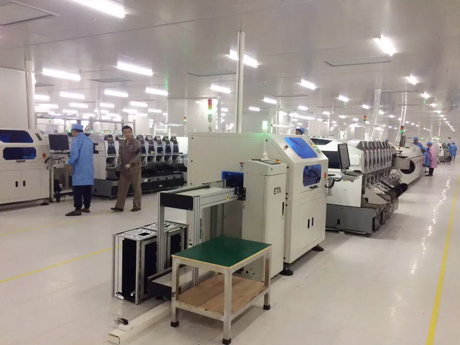
Achieving consistent quality and reliability in PCB printing during mass production is paramount for product success. It necessitates a rigorous approach encompassing robust quality control measures, adherence to stringent testing standards, and the selection of a manufacturer with the appropriate certifications. This ensures that the printed circuit boards not only meet but exceed the performance expectations of the final product.
| Factor | Description | Importance for Mass Production |
|---|---|---|
| Material Selection | Choosing the right substrate and materials that meet performance requirements. | Impacts electrical properties, durability, and overall reliability. |
| Printing Accuracy | Precision in transferring the circuit design onto the substrate. | Directly affects circuit functionality and reduces defects. |
| Etching Quality | Ensuring precise removal of copper to achieve desired traces. | Critical for proper circuit performance and impedance control. |
| Plating Quality | Maintaining uniform plating thickness and adhesion. | Guarantees reliable connections and prevents corrosion. |
| Testing Standards | Rigorous testing according to industry standards. | Validates functionality and long-term reliability of PCBs. |
| Manufacturer Certification | Proof of the manufacturer's adherence to quality standards. | Provides assurance of consistent quality in large volumes. |
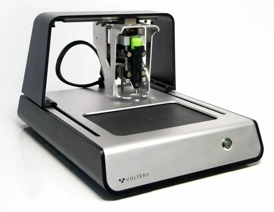
Desktop PCB printing offers a compelling alternative for small-scale projects, enabling a DIY approach to PCB fabrication directly within a workshop or lab environment. This method provides the potential for rapid prototyping and design iteration without relying on external manufacturers, but comes with limitations that must be carefully considered.
Here's a breakdown of the feasibility, practicality, advantages, and limitations of desktop PCB printing:
The suitability of desktop PCB printing is highly dependent on project specifications. Simple circuits, quick prototype boards, and educational designs are well-suited. Projects with complex layouts, high component density, multi-layer requirements, or high precision requirements should typically use professional manufacturing services.
Desktop PCB printer capabilities vary widely. Key specifications to consider include:
| Feature | Description | Implication |
|---|---|---|
| Printing Technology | Inkjet, laser, or CNC milling. | Impacts resolution, precision, and material compatibility. |
| Resolution (DPI) | Dots per inch. | Dictates the smallest track widths and spacing possible. |
| Accuracy | How closely the printer matches the designed layout. | Affects the reliability of the connections. |
| Printing Speed | Rate at which a board can be printed. | Determines the time to fabricate a prototype. |
| Material Compatibility | Types of substrates the printer can handle. | Limited to single sided, double-sided, FR-4 and limited choices of flexible materials. |
| Working Area | Maximum board size that the printer can accommodate. | May not support larger projects. |
| Software Integration | How well the printer interacts with design software. | May require specific software or file formats. |
This section addresses common queries regarding PCB printing, covering essential aspects from minimum order quantities and accepted design files to Design for Manufacturing (DFM) and prevalent design pitfalls. Understanding these FAQs will aid in a smoother and more efficient PCB manufacturing process.
The PCB printing landscape is rapidly evolving, driven by demands for greater flexibility, enhanced performance, and miniaturization. These advancements are paving the way for innovative applications and reshaping electronics manufacturing. Key trends include the adoption of flexible substrates, development of advanced materials, and the emergence of novel printing technologies, all contributing to a more agile and efficient PCB production process.
Understanding the nuances of PCB printing is vital for anyone involved in electronics design and manufacturing. From selecting the right printing method and service to navigating cost and ensuring quality, informed decisions are key to successful projects. The future of PCB printing is bright, with new technologies promising even more efficient, sustainable, and innovative solutions. By staying informed and adaptable, you can leverage PCB printing to bring your projects from concept to reality and make a significant impact in the ever-evolving tech landscape. With advancements in desktop printing and new materials, the possibilities are endless for innovation in various industries and applications.

