Medical Imaging Storage and Transmission PCB Solution
2025.07.31
In the rapidly evolving landscape of healthcare, medical imaging stands as a cornerstone of diagnostics and treatment. The precision, speed, and reliability of medical imaging systems are paramount, directly impacting patient care outcomes. At the heart of these sophisticated machines lies the Printed Circuit Board (PCB), the unsung hero enabling seamless data acquisition, storage, and transmission. This article delves into the critical role of specialized PCB solutions in medical imaging, highlighting how Zero One Solution Limited, a leader in rapid prototyping and one-stop PCB services, empowers medical device manufacturers to overcome design challenges and accelerate innovation in this vital sector.
The Critical Role of PCBs in Medical Imaging
PCB in Medical Imaging Equipment
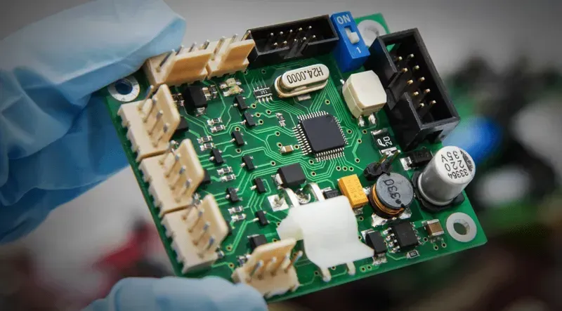
In the advanced landscape of modern healthcare, Printed Circuit Boards (PCBs) are not merely components but the fundamental backbone enabling the precision, speed, and unwavering reliability crucial for medical imaging systems. These sophisticated circuits are the silent architects behind the capture, processing, and transmission of vital diagnostic information, from the intricate details revealed by MRI and CT scans to the real-time insights provided by ultrasound and X-ray devices. The ability of medical imaging PCBs to manage colossal data volumes with exceptional integrity and facilitate real-time processing is paramount, directly impacting diagnostic accuracy, treatment efficacy, and ultimately, patient safety. Without high-performance PCBs, the intricate functionality and life-saving capabilities of contemporary medical imaging technologies would be unattainable.
Accuracy and Precision in Diagnostics PCBs in medical imaging systems must ensure signal integrity and minimal noise interference to accurately capture and reconstruct images. This precision is vital for correct diagnoses, as even slight distortions can lead to misinterpretations of medical conditions. For instance, in an MRI, the PCB controls the timing and intensity of radiofrequency pulses and magnetic gradients, directly influencing image resolution and clarity. Data fidelity from acquisition to display is paramount for clinical confidence and effective patient care.
High-Speed Data Processing and Transmission Modern medical imaging generates immense volumes of data at extremely high rates. For example, a single CT scan can produce gigabytes of data in seconds. PCBs are engineered to handle these high-bandwidth requirements through optimized trace routing, impedance control, and advanced material selection, ensuring rapid image reconstruction and real-time visualization. This speed is critical for reducing scan times, improving patient throughput, and facilitating immediate clinical decisions during examinations or interventions.
Medical Imaging Modality
Key PCB Requirement
Impact on Performance
MRI (Magnetic Resonance Imaging)
High-frequency signal integrity, low noise
Enables high-resolution soft tissue contrast, critical for neurology and oncology
CT (Computed Tomography)
High-speed data processing, power efficiency
Facilitates rapid 3D image reconstruction, crucial for trauma and emergency diagnostics
X-ray & Digital Radiography
Stable power delivery, low-latency data transfer
Ensures clear, high-contrast images for bone and chest pathologies, quick review
Ultrasound
Analog front-end precision, high-channel density
Provides real-time, non-invasive imaging, essential for cardiology and obstetrics
Key Challenges in Medical Imaging PCB Design
High-Speed Signal PCB Routing
Designing Printed Circuit Boards (PCBs) for medical imaging systems presents a unique confluence of technical and regulatory hurdles, demanding a level of precision and reliability far exceeding that of typical electronic devices. At the heart of these challenges lies the imperative for impeccable signal integrity, efficient thermal management, and robust electromagnetic compatibility (EMC), all while navigating stringent regulatory frameworks to ensure patient safety and diagnostic accuracy. These factors collectively define the critical design parameters that differentiate medical imaging PCBs and necessitate specialized expertise.
High-Speed Signal Integrity (SI) Medical imaging devices process enormous volumes of high-resolution data in real-time. Maintaining signal integrity at multi-gigabit speeds is paramount, requiring meticulous impedance control, careful trace routing, and the selection of advanced low-loss dielectric materials to prevent signal degradation, reflections, and crosstalk. Any compromise in SI can lead to image artifacts, diagnostic errors, and ultimately, patient safety concerns.
Thermal Management The miniaturization and increased functionality of medical imaging systems often result in higher power densities and heat generation within compact spaces. Effective thermal management through advanced PCB stack-ups, integrated heat sinks, thermal vias, and careful component placement is crucial to prevent overheating, which can lead to performance degradation, component failure, and reduced device lifespan, impacting device reliability and uptime.
Electromagnetic Compatibility (EMC) Medical environments are highly sensitive to electromagnetic interference (EMI), which can disrupt the operation of critical equipment and compromise image quality. Designing PCBs with robust EMC shielding, proper grounding, filtering, and noise suppression techniques is essential to ensure that medical imaging devices operate reliably without interfering with other medical equipment or being affected by external noise sources. This directly impacts diagnostic precision and patient safety.
High-Density Interconnect (HDI) Technologies To accommodate the increasing complexity and component density of modern medical imaging electronics, HDI technologies, including microvias, build-up layers, and fine-pitch components, are indispensable. HDI enables greater circuit routing capabilities in smaller footprints, crucial for compact portable devices and complex fixed systems, without sacrificing performance or reliability.
Stringent Regulatory Compliance (FDA, ISO 13485) Beyond technical performance, medical imaging PCBs must adhere to rigorous regulatory standards such as FDA (U.S. Food and Drug Administration) regulations and ISO 13485 for medical device quality management systems. Compliance involves strict control over design validation, material traceability, manufacturing processes, risk management, and documentation, ensuring that every PCB meets the highest safety, quality, and performance benchmarks for clinical use. Non-compliance can lead to severe penalties, product recalls, and jeopardize patient trust.
High-Speed Data Transmission PCB Solutions
Medical Imaging Data Transmission PCB
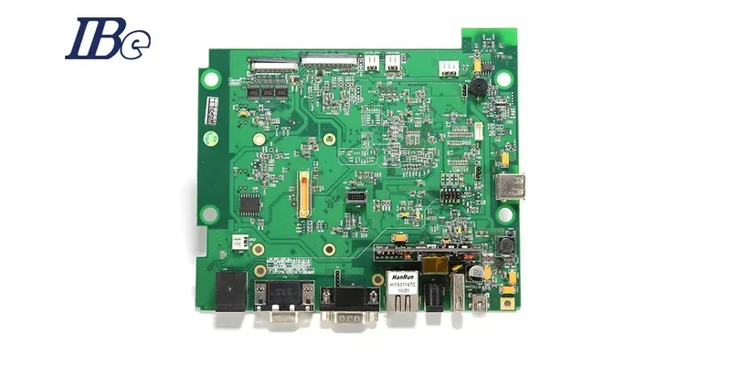
Achieving ultra-fast and impeccably reliable data transmission is paramount for modern medical imaging systems, where even nanosecond delays can compromise diagnostic accuracy or patient outcomes. The foundational element enabling this high-speed data flow is the Printed Circuit Board (PCB), necessitating advanced design strategies and material selections to manage colossal data volumes from modalities like MRI, CT, and ultrasound without signal degradation or latency. This critical component ensures that intricate, high-resolution images are captured, processed, and transmitted with the fidelity required for precise medical analysis.
Controlled Impedance Routing Maintaining precise impedance control across PCB traces is fundamental for high-speed signal integrity. Any impedance mismatch can lead to signal reflections, causing data errors and compromising image quality. Zero One Solution Limited employs sophisticated design tools and manufacturing processes to ensure tight impedance tolerances, critical for differential pairs and single-ended lines in data pathways.
Specialized Laminates with Low Dielectric Loss The choice of PCB laminate material significantly impacts signal attenuation at high frequencies. Traditional FR-4 materials can introduce excessive signal loss. For medical imaging, we utilize advanced laminates such as low-loss FR-4 variants, hydrocarbon ceramics, or PTFE-based materials. These specialized materials exhibit lower dielectric constants (Dk) and dissipation factors (Df), minimizing signal loss and ensuring robust transmission even at multi-gigabit speeds.
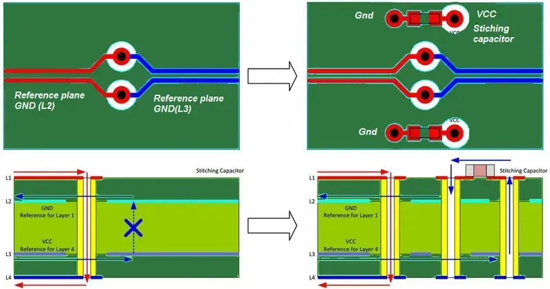
Advanced Via Technologies Vias, while essential for interconnecting layers, can introduce discontinuities that degrade high-speed signals. Our solutions incorporate advanced via technologies like blind vias, buried vias, and microvias to minimize stub length, reduce parasitic capacitance and inductance, and improve signal integrity. This careful via design is crucial for preventing signal reflections and ensuring clean data transmission across multiple layers of complex medical imaging PCBs.
Optimized Stack-Up Design A well-engineered PCB stack-up is vital for both signal integrity and electromagnetic compatibility (EMC). We meticulously design the layer arrangement, including ground and power planes, to provide optimal return paths for high-speed signals, effectively mitigating noise and crosstalk. This structured approach helps in maintaining a stable impedance environment and reducing electromagnetic interference, essential for sensitive medical devices.
Thermal Management Considerations High-speed data transmission often generates significant heat, which can impact component performance and long-term reliability. Our designs integrate effective thermal management strategies, such as incorporating copper pours, thermal vias, and strategic component placement, to dissipate heat efficiently. This ensures that the PCB operates within optimal temperature ranges, preventing performance degradation and extending the lifespan of critical components.
Robust Data Storage PCB Integration
PCB with Integrated Memory Chips
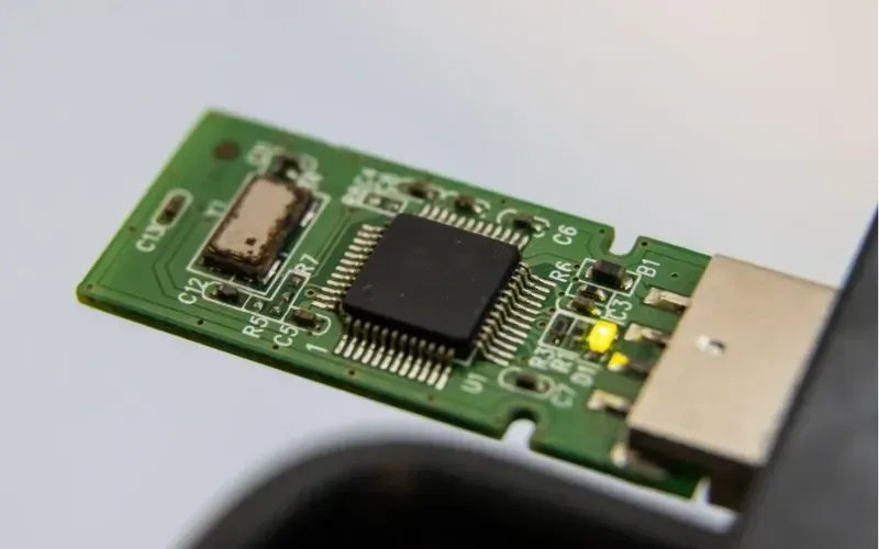
In the realm of medical imaging, the ability to securely and efficiently store vast amounts of high-resolution data is paramount. This necessitates robust PCB integration strategies that prioritize data integrity, rapid access, and unwavering power stability. These PCBs are not merely connectors; they are the backbone supporting the critical functions of data capture, processing, and archival, ensuring that medical professionals have immediate and reliable access to vital diagnostic information.
Memory Type
Key Advantages for Medical Imaging
PCB Integration Considerations
SSDs (Solid State Drives)
High speed read/write, ruggedness, low power consumption, compact size.
Optimized for high-speed interfaces (SATA, NVMe), thermal management for sustained performance, robust power delivery networks.
DDR SDRAM (Double Data Rate Synchronous Dynamic Random Access Memory)
Extremely high bandwidth, ideal for real-time image processing and temporary storage.
Precise impedance matching, careful trace routing for signal integrity, dedicated power rails for stable operation.
Why is power integrity crucial for data storage PCBs? Power integrity ensures that a stable and clean power supply reaches all components, especially memory modules. Fluctuations or noise in power can lead to data corruption, read/write errors, and system instability, which is unacceptable in critical medical imaging applications where data accuracy is paramount. Robust power delivery networks (PDNs) with proper decoupling capacitors and ground planes are essential to mitigate these risks and ensure reliable data storage operations.
Zero One Solution Limited's Expertise in Medical PCB Prototyping
Medical PCB Prototype Manufacturing
Zero One Solution Limited stands as a premier partner in the rapid prototyping of Printed Circuit Boards (PCBs) for the demanding medical imaging sector. Our core competency lies in delivering accelerated R&D prototype manufacturing, enabling clients to dramatically shorten product development cycles and bring innovative medical solutions to market with unparalleled efficiency. We understand that in the realm of medical technology, speed to market combined with uncompromising quality is paramount. Our integrated approach, spanning from meticulous PCB design to advanced manufacturing and seamless assembly, is engineered to facilitate swift validation and refinement of critical medical device designs.
Expedited PCB Design and Optimization We offer specialized PCB design services tailored for medical imaging applications, focusing on high-speed signal integrity, thermal management, and miniaturization. Our design engineers leverage decades of experience to optimize layouts for performance and manufacturability, identifying potential issues early to prevent costly delays in prototyping. This includes comprehensive DFM (Design for Manufacturability) and DFA (Design for Assembly) analyses, crucial for medical-grade precision.
Rapid-Response Manufacturing Capabilities Our state-of-the-art manufacturing facilities are equipped for quick-turn PCB fabrication, utilizing advanced materials and processes suitable for stringent medical requirements. From single-layer boards to complex multi-layer HDI designs, we ensure rapid turnaround times without compromising on quality or adherence to ISO 13485 standards. This agility is vital for iterative design processes in R&D.
Capability
Benefit for Medical Prototyping
Impact on R&D
High-Speed Material Sourcing
Access to low-loss laminates and specialized substrates critical for medical imaging signal integrity.
Enables true-to-design performance validation, reducing prototype iterations due to material limitations.
Precision Assembly and Testing Beyond manufacturing, Zero One Solution Limited provides comprehensive PCB assembly services, including SMT, Through-Hole, and advanced package assembly for medical devices. Each assembled board undergoes rigorous testing, including AOI, X-ray inspection, and functional testing, to ensure every component functions as intended and meets the highest performance and reliability benchmarks required for medical applications. This stringent QA process accelerates validation, ensuring that prototypes are robust and reliable for critical clinical trials.
Quality Assurance and Reliability in Medical PCB Manufacturing
In the realm of medical imaging, the performance and longevity of devices are paramount, directly impacting patient safety and diagnostic accuracy. This underscores the critical importance of stringent quality assurance and unwavering reliability in the manufacturing of medical PCBs. Zero One Solution Limited is deeply committed to upholding the highest standards, integrating rigorous testing, meticulous material selection, and strict adherence to global industry standards into every stage of our PCB production process.
Aspect of Quality
Zero One Solution Limited's Approach
Benefits for Medical Imaging
Industry Standards Compliance
ISO 13485, IPC Class 2/3, FDA guidelines (where applicable)
Ensures regulatory acceptance and patient safety
Rigorous Testing Procedures
AOI (Automated Optical Inspection), X-ray Inspection, Flying Probe Testing, In-Circuit Test (ICT), Functional Test (FCT)
Detects microscopic defects, verifies electrical integrity, and confirms functional performance
Advanced Material Selection
Biocompatible laminates, low-loss dielectrics, high Tg materials
Ensures signal integrity, thermal stability, and long-term device durability
Traceability and Documentation
Comprehensive batch tracking and detailed manufacturing records
Facilitates rapid issue resolution and compliance auditing
Environmental Control
Cleanroom environments, controlled humidity and temperature
Minimizes contamination and optimizes manufacturing consistency
Our comprehensive approach to quality and reliability goes beyond mere compliance; it's an intrinsic part of our engineering philosophy. By employing state-of-the-art inspection technologies and adhering to a zero-defect mindset, we ensure that every PCB delivered for medical imaging applications is not only high-performing but also inherently safe and reliable, contributing directly to the precision and trustworthiness of medical diagnostics worldwide.
Customized Solutions for Diverse Medical Imaging Modalities
Zero One Solution Limited excels in delivering highly customized PCB solutions, precisely engineered to meet the unique demands of various medical imaging modalities. Recognizing that each modality, from the intricate requirements of high-resolution MRI systems to the portability needs of ultrasound devices and the complex data processing of advanced computed tomography (CT) scanners, presents distinct challenges, we offer adaptable design and manufacturing services. This flexibility ensures optimal performance, reliability, and regulatory compliance for every specialized medical imaging application.
High-Resolution MRI Systems For MRI, where signal integrity and noise reduction are paramount, our customized PCBs feature advanced material laminates with low dielectric loss and precise impedance control. We implement multi-layer designs with optimized grounding and shielding to minimize electromagnetic interference, critical for capturing high-fidelity images and ensuring patient safety in strong magnetic fields. Our solutions support high-speed data acquisition and processing required for detailed anatomical visualization.
Portable Ultrasound Devices Portable ultrasound devices demand compact, lightweight, and power-efficient PCB solutions. We specialize in High-Density Interconnect (HDI) PCBs, utilizing fine lines and microvias to maximize component density while maintaining signal integrity. Our designs prioritize low power consumption and efficient thermal dissipation, crucial for extending battery life and ensuring stable operation in a portable form factor, often integrating flexible PCB technology for ergonomic designs.
Advanced Computed Tomography (CT) Scanners CT scanners require robust PCBs capable of handling massive data throughput and complex algorithmic processing for image reconstruction. Our solutions incorporate advanced high-speed routing techniques, specialized cooling mechanisms, and power integrity networks to support continuous, high-performance operation. We leverage multi-gigabit transceivers and high-capacity memory interfaces to manage the real-time data streams from detectors and deliver rapid image generation for clinical diagnostics.
FAQs about Medical Imaging PCB Solutions
Navigating the complexities of Medical Imaging PCB Solutions requires a deep understanding of design, manufacturing, and stringent regulatory compliance. This FAQ section addresses common inquiries, offering clear, concise answers to help engineers and product developers optimize their medical imaging device projects, ensuring optimal performance, reliability, and patient safety.
What are the primary considerations for high-speed signal integrity in Medical Imaging PCBs? Achieving high-speed signal integrity in medical imaging PCBs is critical due to the massive data volumes and real-time processing demands. Key considerations include careful impedance matching (typically 50-ohm differential pairs), minimizing crosstalk through proper trace spacing and shielding, selecting low-loss dielectric materials (e.g., high-Tg laminates, PTFE-based materials), and optimizing via design to reduce inductance and capacitance. Utilizing signal integrity analysis tools during the design phase is paramount to predict and mitigate potential issues before fabrication, ensuring signal fidelity and preventing data corruption in sensitive medical data acquisition systems like MRI and CT scanners.
How do Medical Imaging PCBs address thermal management challenges? Medical imaging PCBs often generate significant heat due to high-speed processing and power demands. Effective thermal management is essential to prevent performance degradation and ensure long-term reliability. Strategies include incorporating thermal vias to dissipate heat to ground planes, utilizing thick copper layers for improved thermal conductivity, integrating heat sinks or active cooling solutions (fans, liquid cooling) directly onto the PCB, and selecting substrate materials with superior thermal performance. Advanced thermal simulation tools are used during design to identify hotspots and optimize heat dissipation pathways, ensuring components operate within safe temperature limits and extending device lifespan.
What regulatory standards apply to Medical Imaging PCBs? Medical Imaging PCBs must adhere to rigorous regulatory standards to ensure patient safety and device efficacy. Key standards include ISO 13485 (Quality Management Systems for Medical Devices), IEC 60601 (Medical Electrical Equipment - General Requirements for Basic Safety and Essential Performance), and FDA regulations (21 CFR Part 820 for Quality System Regulation) in the United States. Compliance involves meticulous documentation, stringent material traceability, controlled manufacturing processes, and comprehensive testing to meet electromagnetic compatibility (EMC/EMI) and safety requirements. Partnering with a PCB manufacturer experienced in medical device compliance is crucial for navigating these complex regulatory landscapes.
Why is material selection critical for Medical Imaging PCB reliability? Material selection is paramount for medical imaging PCB reliability due to demanding operational environments and long product lifecycles. High-performance laminates with stable dielectric constants (Dk) and low dissipation factors (Df) are necessary for high-frequency signal transmission, minimizing signal loss and ensuring precise image acquisition. Materials must also exhibit excellent thermal stability to withstand temperature cycling, robust mechanical properties for durability, and chemical resistance. Furthermore, biocompatible and lead-free materials are often required, aligning with environmental regulations and patient contact safety, particularly for devices with direct or indirect patient interaction. The right material ensures signal integrity, thermal stability, and overall device longevity.
The future of medical imaging hinges on advancements in underlying technologies, with PCB solutions playing an indispensable role. Zero One Solution Limited is committed to being at the forefront of this evolution, offering bespoke, high-performance PCB design, manufacturing, and assembly services that meet the stringent demands of the medical industry. Our expertise ensures reliable data storage, ultra-fast transmission, and robust system integrity, enabling the development of next-generation medical imaging devices. Partner with Zero One Solution Limited to transform your innovative medical imaging concepts into market-ready realities. Contact us today to discuss your specific PCB solution needs and accelerate your product development lifecycle.