The mobile PCB board, a marvel of modern engineering, is the unsung hero powering our smartphones. These intricate circuit boards are the foundation upon which all mobile device functionality is built, interconnecting thousands of tiny components that enable us to communicate, access the internet, and so much more. This article dives deep into the world of mobile PCB boards, exploring their various types, designs, key components, and manufacturing processes to provide you with a complete understanding of this crucial element in mobile technology.
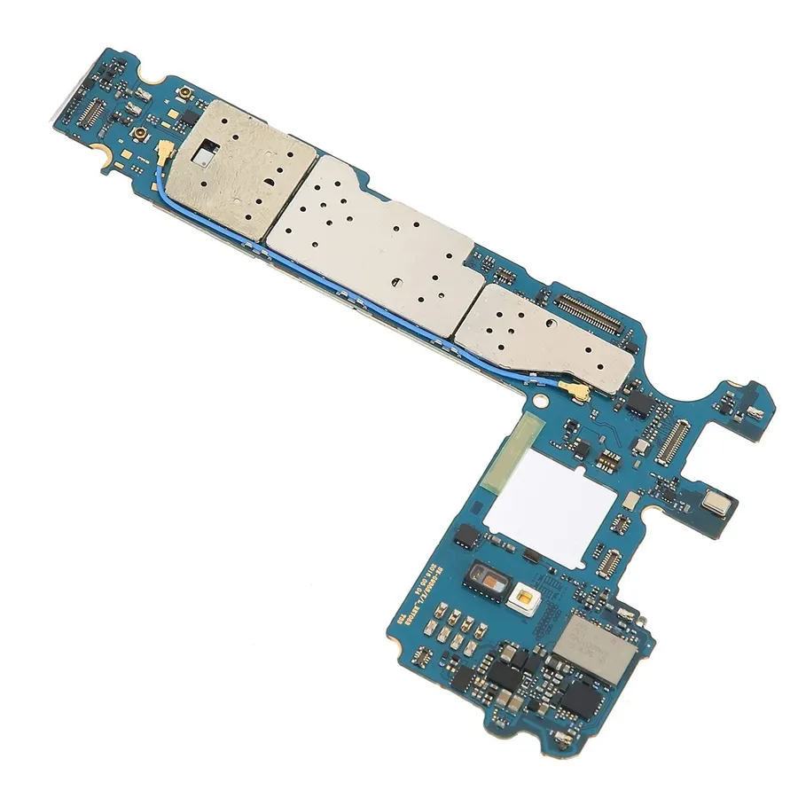
A mobile Printed Circuit Board (PCB) is the foundational component within a smartphone, serving as the central platform for mounting and electrically connecting all the electronic parts. This multi-layered board facilitates the intricate communication and power distribution necessary for a mobile device's functionality, essentially acting as its nervous system, and allowing all the individual components to work together seamlessly to deliver a functional product.
The mobile PCB is critical to the operation of a smartphone because it ensures both structural support for all electrical components and provides the electrical pathways required for signal transmission and power delivery. Without it, the mobile phone could not exist or function.
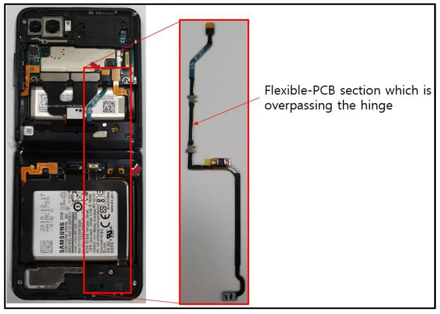
Mobile devices employ various types of Printed Circuit Boards (PCBs), each tailored to specific needs and design constraints. These PCBs primarily fall into three categories: rigid, flexible, and rigid-flex. The selection of PCB type is crucial for optimizing performance, space utilization, and overall device functionality. Understanding the characteristics of each type is essential for designing and manufacturing efficient mobile devices.
| Type | Description | Advantages | Disadvantages | Typical Applications |
|---|---|---|---|---|
| Rigid PCBs | Made from solid, inflexible materials like FR-4. Commonly multi-layered for complex circuitry. | Cost-effective, durable, high component density possible, well-established technology. | Limited flexibility, prone to damage from bending, can be bulky. | Main logic board, power management sections, areas with minimal movement. |
| Flexible PCBs | Constructed from thin, flexible substrates like polyimide. Capable of bending and flexing without damage. | Lightweight, compact, excellent bending capabilities, high design freedom, good for high-density interconnects. | More expensive than rigid PCBs, less durable, complex assembly required. | Connecting cameras to main board, display connections, buttons, areas requiring flexibility. |
| Rigid-Flex PCBs | Combines rigid and flexible sections in one PCB. Integrates the benefits of both types. | Integrates rigid and flexible sections which reduces the need for connectors, offers design flexibility, reliable connection, space-saving. | High cost, complex manufacturing process, design challenges. | Complex interconnections between multiple sections, devices with multiple moving parts. |
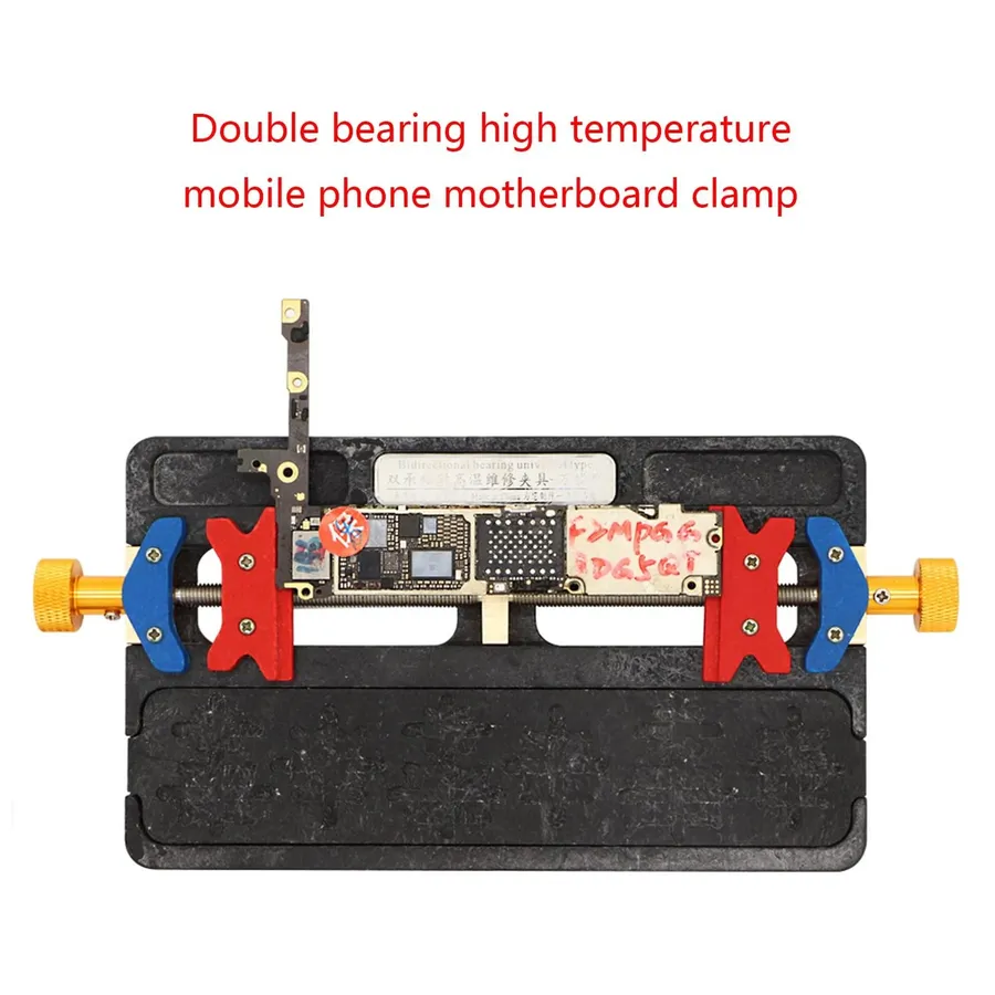
The mobile PCB (Printed Circuit Board) is the central hub of a smartphone, housing numerous critical components that dictate its functionality. These components work synergistically to enable communication, processing, storage, and user interaction. Understanding these key elements and their arrangement is essential for comprehending the overall operation and performance of a mobile device.
| Component | Function | Impact of Placement |
|---|---|---|
| Application Processor (AP) | The 'brain' of the phone; executes instructions, handles calculations, and manages overall device operations. | Central placement on the PCB to optimize thermal dissipation and minimize signal delays to connected peripherals. |
| RAM (Random Access Memory) | Provides temporary data storage for active applications and processes, enabling quick access for the AP. | Proximity to the AP is vital to maximize data transfer speed and minimize latency, often directly connected. |
| ROM (Read Only Memory) | Stores the device's firmware, operating system, and other essential data, retaining information even when the power is off. | Usually placed to minimize interference with active circuits, but close enough for efficient booting. |
| Power Management IC (PMIC) | Regulates power distribution to all components, managing charging, battery health and optimizing battery life. | Strategically located near the battery connector and other power-hungry components to minimize loss and maintain voltage integrity. |
| Connectivity Modules (Wi-Fi, Bluetooth, Cellular) | Enable wireless communication via various protocols for network access and data exchange. | Positioned to avoid interference between modules and with other high-frequency signals, often near the antenna feeds. |
| Sensors (Accelerometer, Gyroscope, Magnetometer) | Detect device orientation, motion, and environmental conditions, enabling user-interface and application functionality. | Placed at locations to enable accurate data collection, often situated at the edges or corners of the board for spatial sensitivity. |
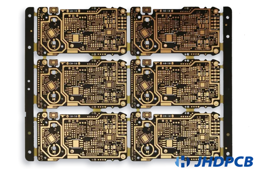
Mobile printed circuit boards (PCBs) are typically multi-layered structures, designed to optimize space and performance within compact mobile devices. The selection of materials and the number of layers are critical factors influencing the overall functionality and reliability of the mobile phone.
| Layer Type | Typical Material | Function | Thickness Range |
|---|---|---|---|
| Core Layer(s) | FR-4 (Fiberglass Reinforced Epoxy) or Polyimide | Provides structural support and insulation between conductive layers. | 50 μm - 200 μm |
| Copper Layer(s) | Copper | Forms the conductive traces, pads, and planes for signal and power distribution. | 10 μm - 35 μm |
| Prepreg Layer(s) | Epoxy resin with fiberglass or other reinforcing material | Bonds core and copper layers together and provides insulation. | 25 μm - 100 μm |
| Solder Mask Layer(s) | Epoxy-based polymer | Protects conductive traces from oxidation, corrosion, and short circuits and facilitates solderability. | 10 μm - 25 μm |
| Silkscreen Layer(s) | Epoxy ink | Provides component identification, polarity markings, and test points on the PCB. | 5 μm - 10 μm |
The number of layers in a mobile PCB can range from 4 to 12 or more, depending on the complexity of the device and its required functionality. Higher layer counts allow for more intricate routing, improved signal integrity, and better power distribution. Common layer configurations include 4-layer, 6-layer, and 8-layer PCBs. The materials are carefully selected to provide a balance between mechanical strength, electrical properties, thermal performance, and cost.
Copper traces are essential for electrical connectivity within mobile PCBs. These thin conductive lines, formed by etching a copper layer, facilitate the flow of electrical signals and power between components. Trace width and spacing are carefully designed to ensure signal integrity, minimize interference, and handle the required current load. The thickness of the copper layer impacts current carrying capacity, with thicker copper being used for power traces and thinner copper being used for signal traces.
Material selection is paramount for performance and reliability. FR-4 is widely used because of its cost-effectiveness, good mechanical strength, and electrical properties. Polyimide is a premium material used in high-performance mobile devices because of its superior thermal stability, flexibility, and high electrical resistance. The performance of the board can be affected by the material and layer selection, especially the high-frequency signal propagation and thermal management.
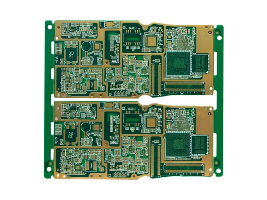
Effective mobile PCB design hinges on several critical factors that directly influence the performance and reliability of the final product. These considerations include miniaturization, signal integrity, thermal management, and power consumption, each demanding careful attention to achieve optimal device functionality within the constraints of a compact mobile form factor.
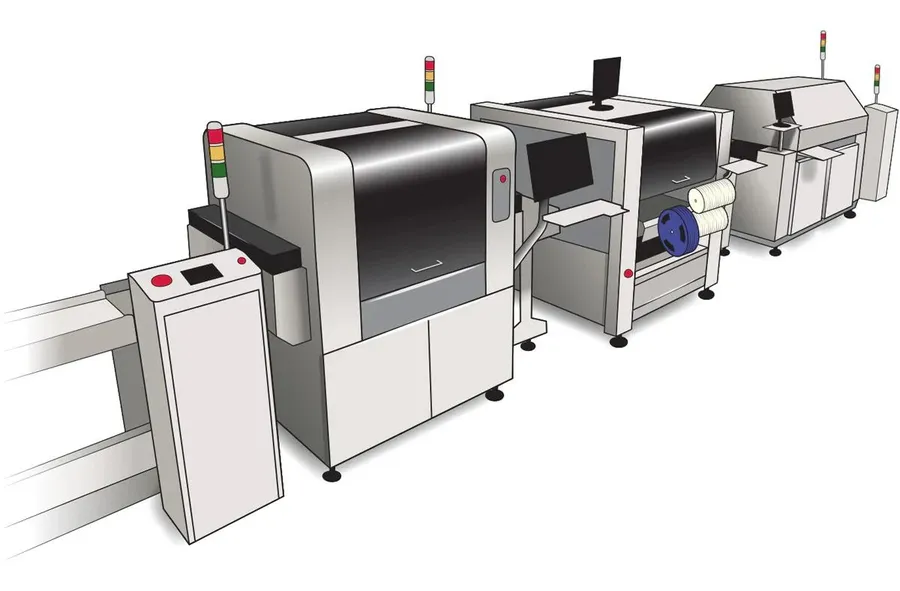
The fabrication of mobile PCB boards is a complex, multi-stage process requiring high precision and adherence to strict quality controls. This process transforms raw materials into the intricate circuit boards that are the heart of mobile devices. Each step is crucial to ensure the performance and reliability of the final product.
Rigorous testing and quality control are paramount in ensuring the reliability and performance of mobile PCB boards. These processes verify that the manufactured boards meet stringent specifications and operate correctly under various conditions, guaranteeing the overall quality of mobile devices. Comprehensive testing procedures prevent defects, ensuring that the PCB will support the intended lifespan of the mobile phone.
The following table details common testing procedures for mobile PCB boards:
| Test Type | Description | Purpose |
|---|---|---|
| Electrical Testing | Includes continuity testing, impedance testing, and shorts testing. | Verifies electrical connections, ensuring that signals flow correctly and that there are no unintended shorts or opens. |
| Functional Testing | Simulates real-world operating conditions using specialized testing fixtures and software. | Confirms that all components on the PCB function correctly and interact as designed under realistic operational conditions. |
| Visual Inspection | Detailed examination of the PCB using microscopes and cameras. | Checks for physical defects such as cracks, solder joint issues, misaligned components, and any surface contamination. |
| X-Ray Inspection | Uses X-ray technology to examine internal layers and components | Identifies hidden defects within the PCB structure or under BGA components that are not visible with standard visual inspection. |
| Environmental Testing | Subjects PCBs to extreme temperature, humidity, and vibration conditions. | Determines the boards' ability to withstand challenging environmental conditions over their expected lifespan. |
Mobile PCB boards must conform to specific industry standards to ensure safety and reliability. These standards provide guidelines for material selection, manufacturing processes, and performance criteria. Adherence to these standards is a prerequisite for the boards to be used in consumer electronics. Common Standards include IPC-A-600 which defines acceptable quality for PCBs and is the industry standard used by most manufacturers and PCB designers.
This section addresses common queries regarding mobile PCB boards, offering clear and concise answers to enhance understanding of their role and function in mobile devices.
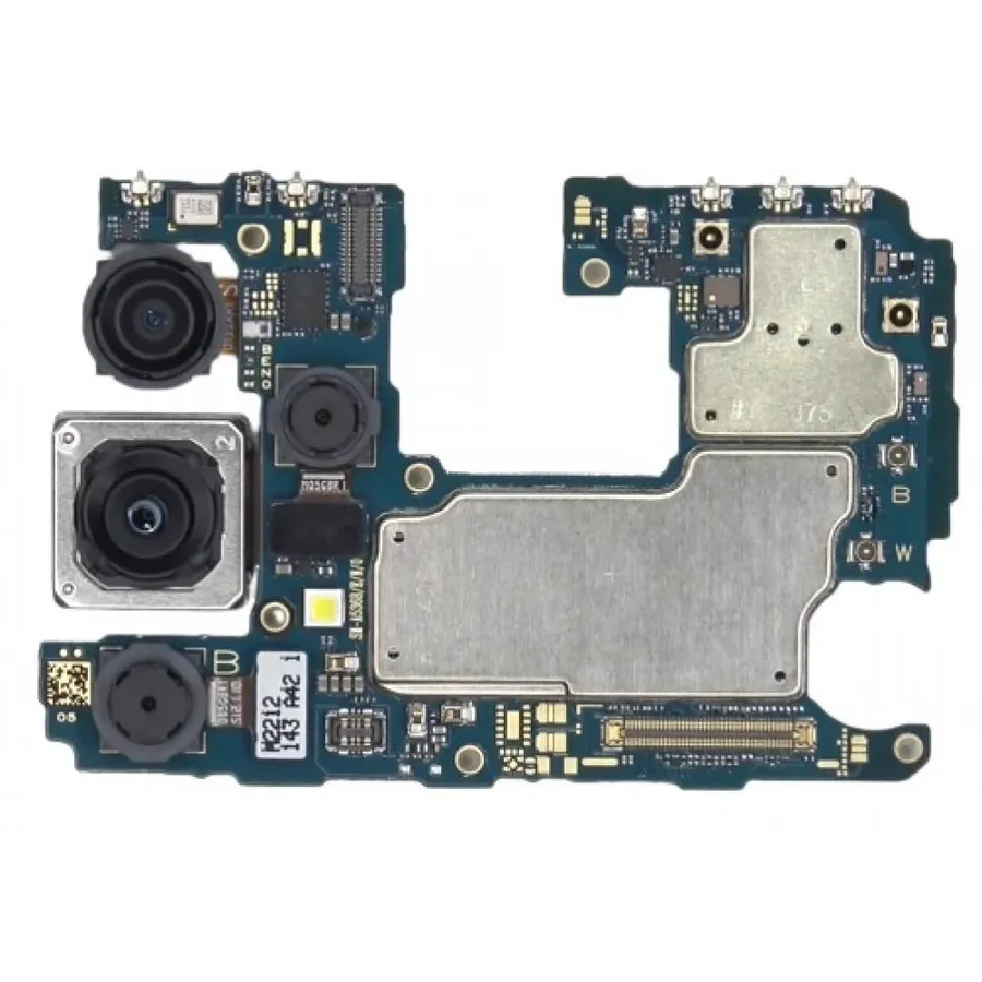
The mobile PCB industry is in constant evolution, driven by the relentless demand for smaller, faster, and more efficient devices. Future trends in mobile PCB technology are focused on addressing these demands through advanced materials, innovative interconnect solutions, and enhanced compatibility with emerging communication standards.
The mobile PCB board is a complex and integral part of any mobile device. Understanding its design, components, and manufacturing is crucial for appreciating the technological marvel that fits in our pockets. From supporting critical components and enabling electrical connections to managing power and performance, the mobile pcb board is a vital foundation. As technology continues to evolve, mobile PCB boards will undoubtedly continue to push the boundaries of what’s possible in the palm of our hands. With advancements in materials, design and manufacturing, we can expect even smaller, more powerful, and more efficient mobile devices in the future, all anchored by the humble, yet essential, mobile pcb board.

