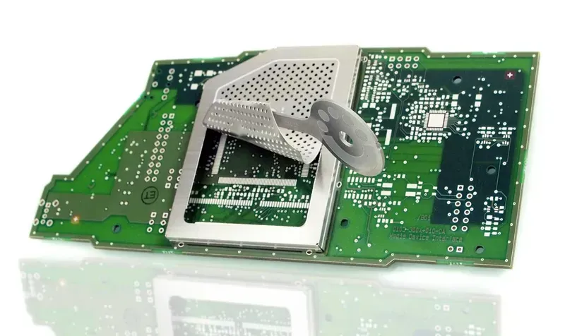
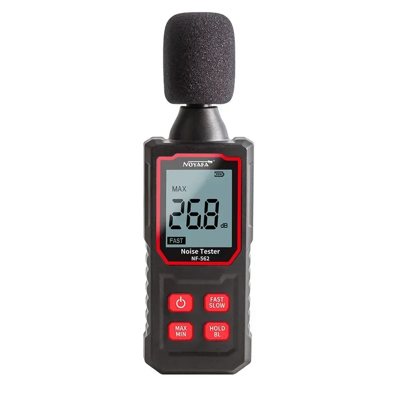
In today's electronic-driven world, noise pollution within systems is a growing concern. From sensitive medical devices to high-performance audio equipment, unwanted noise can significantly impact performance and reliability. At Zero One Solution Limited, we understand the critical importance of minimizing noise in electronic systems. That's why we offer specialized PCB solutions designed specifically for noise control. We leverage our expertise in PCB design, manufacturing, and assembly to provide solutions that mitigate noise, ensuring optimal performance for your products. How do we achieve effective noise control through PCB design? Let's delve into the world of Noise Control System PCB solutions and explore the techniques and best practices that make it possible.
Understanding Noise in Electronic Systems
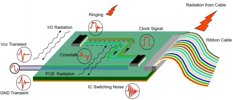
In the intricate world of electronic systems, noise is an omnipresent challenge that can significantly degrade performance, compromise signal integrity, and even lead to system failures. Effectively understanding and mitigating various forms of noise is paramount for designing robust and reliable Printed Circuit Boards (PCBs). This section delves into the fundamental types of noise encountered in electronic systems, examining their origins and the critical impact they have on circuit functionality, laying the groundwork for effective noise control strategies.
Electromagnetic Interference (EMI) EMI is a pervasive form of noise generated by electromagnetic fields that disrupt the operation of electronic devices. It can manifest as conducted EMI, traveling through power lines and signal traces, or radiated EMI, propagating through the air. Common sources include switching power supplies, high-speed digital signals, and even external environmental factors. EMI's impact ranges from minor signal distortion to complete system malfunction, necessitating rigorous design practices to maintain signal integrity and ensure regulatory compliance like FCC and CE standards. A study by IHS Markit projected the global EMI shielding market to reach $7.5 billion by 2025, underscoring the widespread challenge it presents in electronics manufacturing and the increasing demand for effective mitigation solutions.
Radio Frequency Interference (RFI) RFI is a specific type of EMI that occurs within the radio frequency spectrum (typically above 30 kHz). It originates from sources such as wireless communication devices, radio transmitters, and even poorly shielded electronic components. RFI can severely affect sensitive radio receivers, communication links, and high-frequency analog circuits, leading to reduced range, data corruption, or complete loss of signal. Effective RFI suppression is crucial for applications like medical devices, aerospace systems, and telecommunications equipment where signal clarity and reliability are non-negotiable.
Crosstalk Crosstalk is the undesired coupling of energy from one signal trace to an adjacent trace on a PCB. This phenomenon occurs due to mutual capacitance and inductance between closely routed traces, where a changing current or voltage in one trace induces a corresponding voltage or current in another. Factors influencing crosstalk severity include trace spacing, length, signal rise/fall times, and the dielectric constant of the PCB material. Crosstalk can lead to false triggering, timing errors, and reduced signal-to-noise ratio, particularly in high-speed digital designs. For instance, in a 10Gbps Ethernet application, a 5% crosstalk can lead to a significant bit error rate (BER), making meticulous trace routing and impedance control vital.
Beyond these primary noise types, other forms such as thermal noise (due to random electron motion), shot noise (from discrete charge carriers), and flicker noise (low-frequency noise, also known as 1/f noise) also contribute to overall system noise. Understanding these diverse noise sources and their unique characteristics is the initial step towards implementing effective PCB design and manufacturing strategies to ensure superior performance and reliability in noise-sensitive electronic systems.
PCB Design Techniques for Noise Reduction
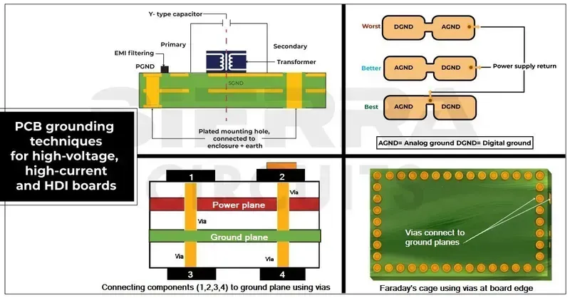
PCB Grounding Techniques
Effective noise reduction in electronic systems hinges significantly on meticulous PCB design. By strategically implementing advanced design techniques, engineers can proactively mitigate electromagnetic interference (EMI) and other forms of noise at the foundational level, ensuring optimal signal integrity and system performance. These techniques are critical for developing robust and reliable electronic products in today’s high-frequency environments.
Grounding Techniques Proper grounding is paramount for noise control. Single-point grounding, ideal for low-frequency circuits, connects all circuit grounds to one common point to prevent ground loops. Multi-point grounding, suitable for high-frequency applications, uses a large ground plane to provide a low-impedance path to ground, minimizing inductance. Star grounding, a hybrid approach, combines elements of both, often used in mixed-signal designs to isolate sensitive analog grounds from noisy digital grounds. Each method aims to establish a stable reference voltage and channel noise away from sensitive components, reducing common-mode noise and crosstalk.
Power Plane Design The design of power planes directly impacts noise propagation. Decoupling capacitors are strategically placed close to IC power pins to provide localized energy storage, suppressing transient current demands and high-frequency noise. Impedance matching within power planes, achieved through careful trace width, length, and dielectric constant selection, ensures efficient power delivery and minimizes reflections that can generate noise. A well-designed power distribution network (PDN) is crucial for stable voltage supply and reduced power-related noise.
Signal Routing Strategies Thoughtful signal routing is essential for maintaining signal integrity and reducing crosstalk. Differential pairs, where two traces carry signals that are equal and opposite, inherently reject common-mode noise due to their symmetrical nature. Controlled impedance routing ensures that transmission lines maintain a consistent characteristic impedance, preventing reflections that can corrupt signals. Minimizing trace lengths, avoiding sharp bends, and maintaining proper spacing between traces also contribute significantly to reducing signal interference and improving overall noise immunity.
Material Selection for Noise Control
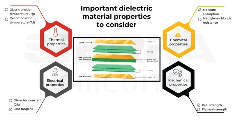
PCB Material Dielectric Properties
The choice of PCB material is not merely a structural consideration; it is a fundamental determinant in the effectiveness of noise control within electronic systems. Beyond mechanical integrity, a material's dielectric properties and shielding effectiveness directly influence signal propagation, impedance control, and the mitigation of electromagnetic interference (EMI) and radio frequency interference (RFI). Selecting the optimal substrate and associated materials is paramount to achieving robust noise immunity and ensuring the long-term reliability and performance of high-frequency or sensitive circuitry.
Material Property
Impact on Noise Control
Common Materials
Dielectric Constant (Dk)
Influences signal propagation speed and impedance. Lower Dk often means faster signals and reduced signal loss, critical for high-frequency noise suppression.
Indicates material's energy loss at high frequencies. Lower Df reduces signal attenuation and heat generation, crucial for maintaining signal integrity and minimizing noise.
Ability to attenuate electromagnetic fields. Materials with good conductive layers or specific compositions can block external noise and prevent internal noise radiation.
Affects heat dissipation. While not directly for noise, efficient heat removal prevents thermal noise and component performance degradation.
Aluminum-backed PCBs, Ceramic substrates
Moisture Absorption
High absorption can alter Dk/Df, leading to performance drift and increased noise sensitivity over time, especially in humid environments.
Standard FR-4 (higher absorption), Low-absorption specialized laminates
Why is material dielectric constant (Dk) important for noise control? A material's dielectric constant directly affects the characteristic impedance of traces and the propagation speed of signals. In high-frequency applications, a consistent and well-controlled impedance is crucial for preventing signal reflections, which are a major source of noise. Materials with a lower and more stable Dk, such as some PTFE-based laminates (e.g., Rogers series), minimize signal distortion and ensure more predictable signal propagation, thus contributing significantly to reduced noise levels and improved signal integrity. Inconsistent Dk across the board or variations with frequency can lead to impedance mismatches and increased noise generation.
By meticulously considering these material properties, Zero One Solution Limited designs and manufactures PCBs that are inherently resistant to noise, ensuring optimal performance for even the most demanding applications.
EMC/EMI Considerations in PCB Layout
PCB Layout EMC Testing
Electromagnetic Compatibility (EMC) and Electromagnetic Interference (EMI) are critical considerations in modern PCB design, dictating a product's ability to function as intended within its electromagnetic environment without causing or succumbing to undue interference. Achieving EMC compliance is not merely a regulatory hurdle but a fundamental aspect of ensuring system reliability, performance, and safety. A poorly designed PCB can act as an unintentional antenna, emitting noise that disrupts other devices or, conversely, become susceptible to external electromagnetic fields, leading to signal integrity issues or operational failures.
Aspect
EMC (Electromagnetic Compatibility)
EMI (Electromagnetic Interference)
Definition
The ability of electronic equipment to function satisfactorily in its electromagnetic environment without introducing intolerable electromagnetic disturbances to anything in that environment.
Any electromagnetic phenomenon that may degrade the performance of a device, equipment, or system, or adversely affect living or inanimate matter. EMI can be both a source and a victim.
][
Focuses on both emissions (the noise a device produces) and immunity (how a device tolerates external noise).
Primarily concerns the unwanted electromagnetic energy generated by a device.
][
Aims for harmonious coexistence of electronic systems.
Aims to mitigate or prevent the harmful effects of electromagnetic noise.
][
Ensures a product meets regulatory standards for operation.
Identifies and addresses specific noise sources and their propagation paths.
Strategic Component Placement Place high-speed components and sensitive analog circuits away from noisy digital sections. Decoupling capacitors should be placed as close as possible to the power pins of ICs to minimize loop inductance and effectively suppress high-frequency noise. Maintain proper spacing between traces to reduce crosstalk, following the 3W rule (trace-to-trace spacing should be at least three times the trace width) for critical signals.
Effective Grounding Schemes Utilize a solid ground plane to provide a low-impedance return path for signals and power. This minimizes ground bounce and noise propagation. For mixed-signal boards, employ a single-point ground connection between analog and digital ground planes to prevent noise coupling while maintaining distinct return paths within each domain.
Power Delivery Network (PDN) Optimization Design a robust PDN with low impedance across a wide frequency range. This involves strategic placement of bulk and high-frequency decoupling capacitors. Use wider power and ground traces or planes to minimize impedance and voltage drops, especially for high-current paths.
Signal Routing Best Practices Route high-speed signals with controlled impedance to prevent reflections and maintain signal integrity. Employ differential pairs for critical high-speed signals to inherently reject common-mode noise. Avoid 90-degree trace bends, as they can cause impedance discontinuities and increase EMI. Keep trace lengths short and minimize loop areas for sensitive signals.
Shielding and Filtering Implementation Consider incorporating shielding techniques such as guard rings around sensitive traces or entire circuit sections. For external interfaces, implement common-mode chokes and ferrite beads to filter out high-frequency noise entering or exiting the PCB. Use appropriate connectors with integrated shielding where necessary to maintain signal integrity across the system boundary.
Adhering to international standards such as CISPR, FCC, and CE is paramount for global market access. For instance, the FCC Part 15 regulations in the US and the CE Mark requirements in Europe set limits on electromagnetic emissions from electronic devices. Compliance often requires rigorous testing in accredited laboratories. Zero One Solution Limited, with its deep expertise in high-frequency PCB design and manufacturing, integrates these EMC/EMI considerations from the conceptual stage, ensuring that your noise-sensitive applications meet stringent regulatory demands while delivering optimal performance and reliability.
PCB Stack-up Design for Improved Signal Integrity
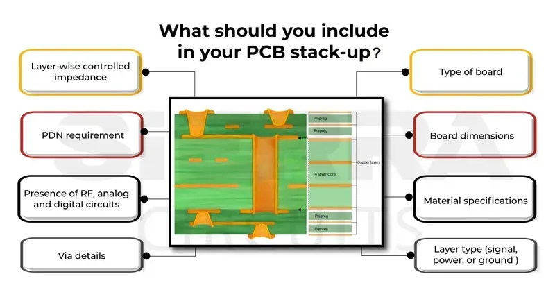
PCB Stack-up Structure
Optimizing PCB stack-up design is paramount for achieving superior signal integrity and effectively mitigating noise in complex electronic systems. A meticulously engineered stack-up provides controlled impedance, minimizes signal reflections, and enhances electromagnetic compatibility (EMC) by creating well-defined return paths for high-frequency signals. This foundational aspect of PCB design directly influences the overall performance and reliability of noise-sensitive applications, from high-speed data transmission to precision analog circuits.
Why is PCB stack-up crucial for signal integrity? PCB stack-up defines the arrangement of conductive layers and insulating dielectric materials. A proper stack-up ensures consistent impedance for signal traces, preventing reflections and signal degradation. It also provides low-impedance return paths, crucial for high-frequency current flow, thereby minimizing electromagnetic interference (EMI) and crosstalk.
What are the common stack-up configurations for noise control? Common configurations include 4-layer, 6-layer, and 8-layer boards. For noise control, it's generally recommended to have signal layers tightly coupled to adjacent ground or power planes. For example, a 4-layer stack-up often uses Signal-Ground-Power-Signal, while a 6-layer might be Signal-Ground-Signal-Power-Ground-Signal, optimizing for both signal integrity and power delivery network (PDN) performance.
How does impedance control relate to stack-up design? Impedance control is fundamentally achieved by carefully selecting dielectric thickness, trace width, and the dielectric constant of the materials within the stack-up. The relationship between these parameters determines the characteristic impedance of signal traces, ensuring signals propagate without significant reflections and maintaining signal integrity, which is vital for noise reduction.
What role do ground and power planes play in stack-up for noise reduction? Dedicated ground and power planes within the stack-up serve as low-impedance return paths for signals and provide stable power distribution. Solid, continuous planes minimize loop areas, reducing inductive effects and preventing noise coupling. They also act as shielding, containing electromagnetic fields and protecting signals from external interference.
What are the risks of a poorly designed PCB stack-up regarding noise? A poor stack-up can lead to uncontrolled impedance, causing signal reflections, ringing, and increased rise/fall times. This results in significant signal integrity issues, higher EMI emissions due to large current loops, crosstalk between adjacent traces, and increased susceptibility to external noise, ultimately degrading system performance and reliability.
Shielding Techniques for PCBs
PCB Shielding Enclosure
Effective shielding is paramount in advanced PCB design, acting as a critical barrier against external electromagnetic interference (EMI) and radio frequency interference (RFI) that can degrade signal integrity and system performance. By strategically enclosing sensitive circuit elements or the entire PCB, shielding techniques prevent both the ingress of unwanted noise and the egress of internally generated emissions, ensuring the reliability and compliance of electronic systems. This proactive approach to noise control is vital for high-performance applications where signal fidelity is non-negotiable.
Metallic Enclosures Metallic enclosures, typically made from aluminum, steel, or copper, provide robust EMI/RFI shielding by reflecting and absorbing electromagnetic waves. Their effectiveness is determined by material conductivity, thickness, and the integrity of seams and openings. Proper grounding of the enclosure to the system's ground plane is crucial to dissipate induced currents and maintain shield effectiveness. These are ideal for complete system protection in harsh electromagnetic environments.
Shielding Cans (Faraday Cages) Smaller, localized shielding cans, often made of thin metal sheets or stamped metal, are used to enclose specific sensitive components (e.g., oscillators, RF modules) or critical circuit sections on a PCB. These miniature Faraday cages prevent crosstalk between adjacent circuits and protect susceptible components from ambient noise. They are particularly effective in high-density designs where board space is at a premium.
Conductive Coatings and Paints Applied directly to plastic enclosures or non-conductive surfaces, conductive coatings and paints imbue them with shielding properties. These coatings, often containing metallic particles like nickel, copper, or silver, create a conductive layer that attenuates electromagnetic waves. They offer a cost-effective and flexible shielding solution for non-metallic housings, providing a continuous conductive path to block interference while maintaining design aesthetics.
Shielding Method
Mechanism
Application
Advantages
Considerations
Metallic Enclosures
Reflection & Absorption
Full system/device
High effectiveness, robust
Weight, cost, ventilation compromises
Shielding Cans
Localized Isolation
Specific components/circuits
Space-efficient, targeted protection
Placement, thermal management
Conductive Coatings
Surface Conductivity
Plastic housings, non-metallic parts
Flexible, cost-effective, lightweight
Durability, adhesion, surface preparation
Gaskets & Fingerstock
Electrical Continuity
Seams, openings, access panels
Maintains shielding effectiveness across gaps
Compression, material compatibility
Grounding
Current Dissipation
All shielding structures
Prevents current buildup, enhances effectiveness
Proper connection, low impedance path
Implementing the correct shielding technique involves a careful balance of effectiveness, cost, and manufacturability. While metallic enclosures offer broad-spectrum protection, localized shielding cans are ideal for isolating specific sensitive components. Conductive coatings provide a lightweight and adaptable solution for non-metallic housings. Integrating these techniques with proper grounding and considering factors like ventilation and accessibility ensures optimal noise attenuation and system reliability. Our expertise at Zero One Solution Limited encompasses the strategic application of these shielding methods, ensuring your PCB designs meet the most stringent noise control requirements.
Testing and Validation of Noise Control Measures
Noise Measurement Equipment
Thorough testing and validation are paramount to ensuring the efficacy of noise control measures in PCB designs. Without rigorous evaluation, even the most meticulously designed circuits can fall short of performance expectations due to unforeseen electromagnetic interference (EMI) or signal integrity issues. Advanced measurement techniques and robust testing methodologies are essential for identifying noise sources, quantifying their impact, and verifying that implemented solutions meet stringent industry standards and operational requirements, thereby ensuring optimal product functionality and reliability.
Measurement Technique
Description
Primary Application for Noise Control
Spectrum Analysis
Analyzes the frequency content of a signal, identifying noise components and their amplitudes across a wide spectrum.
Identifying specific frequencies of EMI/RFI, characterizing broadband noise, and evaluating filter performance.
Measurement Technique
Description
Primary Application for Noise Control
Time-Domain Reflectometry (TDR)
Sends a pulse down a transmission line and analyzes the reflected signal to characterize impedance changes and discontinuities.
Locating signal integrity issues like impedance mismatches, reflections, and crosstalk sources within PCB traces.
Measurement Technique
Description
Primary Application for Noise Control
EMI/EMC Compliance Testing
Evaluates a device's ability to operate without causing or being susceptible to electromagnetic interference, adhering to international standards (e.g., CISPR, FCC).
Ensuring products meet regulatory requirements for electromagnetic compatibility and identifying areas for improvement in shielding and filtering.
Measurement Technique
Description
Primary Application for Noise Control
Near-Field Probing
Uses specialized probes to measure electromagnetic fields close to the PCB surface, pinpointing exact noise radiation sources.
Pinpointing specific noisy components or traces, identifying current loops, and evaluating the effectiveness of localized shielding.
Measurement Technique
Description
Primary Application for Noise Control
Network Analysis (Vector Network Analyzer - VNA)
Measures the scattering parameters (S-parameters) of a circuit to characterize its frequency response, impedance, and signal loss.
Assessing the performance of passive components (e.g., capacitors, inductors) for noise filtering, evaluating transmission line characteristics, and optimizing impedance matching networks.
Zero One Solution's Noise Control System PCB Solutions
At Zero One Solution, we recognize that effective noise control is paramount for the optimal performance and reliability of electronic systems. As a leading PCB solution provider, our comprehensive approach to noise control systems integrates advanced design, precision manufacturing, and meticulous assembly, ensuring your sensitive applications achieve unparalleled signal integrity and electromagnetic compatibility.
Rapid Prototyping for Noise-Sensitive Designs Our specialization in rapid-response R&D prototype manufacturing allows us to quickly iterate and validate noise control strategies. This agile approach significantly reduces development cycles, enabling you to bring cutting-edge, noise-resilient products to market faster, without compromising on performance or reliability. We employ advanced simulation tools and in-house testing to identify and mitigate potential noise issues early in the design phase.
Integrated Design-to-Assembly Expertise From initial PCB layout to final assembly, Zero One Solution offers a seamless, one-stop service that inherently incorporates noise control considerations at every stage. Our engineers are adept at implementing sophisticated grounding schemes, optimized power plane designs, precise impedance matching, and effective shielding techniques, tailored to the specific noise profile of your application. This holistic approach ensures maximum noise suppression and system stability.
Global Supply Chain Advantage Headquartered in Shenzhen, China, and with a branch in Dubai, Zero One Solution leverages a robust global PCBA supply chain network. This strategic positioning provides unparalleled access to a wide array of high-performance materials, including those with superior dielectric properties and shielding effectiveness critical for advanced noise control. Our diversified sourcing ensures quality, cost-effectiveness, and timely delivery for even the most demanding projects.
Comprehensive Testing and Validation Beyond design and manufacturing, we provide rigorous testing and validation services to verify the efficacy of our noise control solutions. Utilizing state-of-the-art equipment for spectrum analysis, EMI/EMC compliance testing, and signal integrity measurements, we ensure that your PCBs meet stringent industry standards and perform flawlessly in real-world operational environments. Our commitment is to deliver solutions that are not just functional, but also robustly resistant to various forms of electronic noise.
Frequently Asked Questions (FAQs) about Noise Control PCB Solutions
Effective noise control in PCB solutions is paramount for ensuring optimal electronic system performance and reliability. Addressing common inquiries about noise control in PCB solutions helps clarify best practices, cost implications, and the overall effectiveness of various mitigation strategies. Zero One Solution Limited offers comprehensive expertise to navigate these complexities, providing robust PCB solutions tailored to minimize noise across diverse applications.
What are the most common types of noise encountered in PCB designs? The most common types of noise in PCB designs include Electromagnetic Interference (EMI), Radio Frequency Interference (RFI), crosstalk, power supply noise, and ground bounce. EMI/RFI often originate from external sources or internal high-frequency signals, while crosstalk occurs due to capacitive or inductive coupling between adjacent traces. Power supply noise and ground bounce are typically caused by fluctuating current demands and imperfect grounding, respectively, impacting signal integrity and overall system stability.
How does PCB stack-up design influence noise control? PCB stack-up design profoundly influences noise control by dictating impedance, controlling signal return paths, and providing effective shielding. A well-designed stack-up, featuring dedicated ground and power planes, can significantly reduce loop areas for high-frequency currents, thereby minimizing EMI radiation and susceptibility. Proper plane separation and strategic layer assignments help manage crosstalk and ensure stable power delivery, crucial for noise-sensitive circuits. For instance, burying high-speed signal layers between ground planes offers inherent shielding.
Are there cost-effective noise control solutions for budget-constrained projects? Yes, cost-effective noise control solutions exist for budget-constrained projects. While advanced techniques can be costly, fundamental design practices like optimized grounding schemes (e.g., star grounding for sensitive analog circuits), careful trace routing to avoid parallelism and sharp bends, and strategic placement of decoupling capacitors are highly effective and add minimal cost. Utilizing common-mode chokes or ferrite beads on power lines and signal paths can also provide significant noise reduction at a reasonable expense. Prioritizing critical noise sources early in the design phase is key to efficient and economical mitigation.
What role do materials play in achieving effective noise control on PCBs? Materials play a crucial role in effective noise control on PCBs, primarily through their dielectric properties and shielding capabilities. Low-loss dielectric materials (e.g., FR-4 with controlled Df/Dk) reduce signal attenuation and distortion at higher frequencies, indirectly minimizing signal integrity issues that can manifest as noise. Materials with good conductive properties for ground planes improve current return paths, reducing ground bounce. Additionally, specialized materials like shielding films or laminates with embedded ground layers can provide direct EMI/RFI suppression by creating Faraday cages or absorbing electromagnetic energy, essential for sensitive applications.
In conclusion, effective noise control in electronic systems is paramount for ensuring optimal performance and reliability. Zero One Solution Limited stands at the forefront of providing comprehensive PCB solutions designed to minimize noise and maximize signal integrity. From meticulous PCB layout techniques to advanced material selection and rigorous testing, we employ a holistic approach to address noise-related challenges. Partner with Zero One Solution Limited for your next project and experience the difference that expertly designed and manufactured PCBs can make. Contact us today to discuss your specific requirements and let us help you achieve superior performance and reliability in your electronic systems.