In the world of electronics, the NPN BJT transistor is akin to a microscopic gatekeeper, controlling the flow of electrical current with precision. Like a water tap regulating water flow, this three-terminal semiconductor device is at the heart of countless electronic systems, from simple switches to complex amplifiers. This article will unravel the mysteries of the NPN BJT transistor, exploring its fundamental operation, key characteristics, and wide-ranging applications, bridging the gap between fundamental theory and real-world usage.
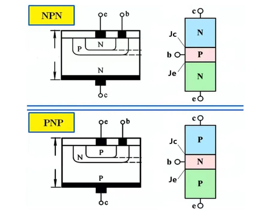
The NPN Bipolar Junction Transistor (BJT) is a three-terminal semiconductor device distinguished by its layered structure comprising two N-type regions separated by a P-type region. This arrangement of N-P-N layers is crucial for the transistor's function as a current-controlled switch or amplifier, with its behavior dictated by the characteristics of the materials and their interfaces.
The N-type regions, referred to as the collector and emitter, are fabricated using semiconductor materials like silicon doped with elements from Group V (e.g., phosphorus or arsenic). These dopants introduce free electrons into the material's crystal lattice, enabling electrical conductivity. The P-type region, called the base, uses semiconductor material such as silicon doped with elements from Group III (e.g., boron or gallium), which creates a deficiency of electrons or “holes”, which also enable conductivity. The interaction of electrons and holes at the junctions between the N and P layers forms the basis for the transistor's operation.
| Layer | Type | Material | Dopant | Charge Carrier |
|---|---|---|---|---|
| Emitter | N-type | Silicon (Si) | Phosphorus (P) or Arsenic (As) | Electrons |
| Base | P-type | Silicon (Si) | Boron (B) or Gallium (Ga) | Holes |
| Collector | N-type | Silicon (Si) | Phosphorus (P) or Arsenic (As) | Electrons |
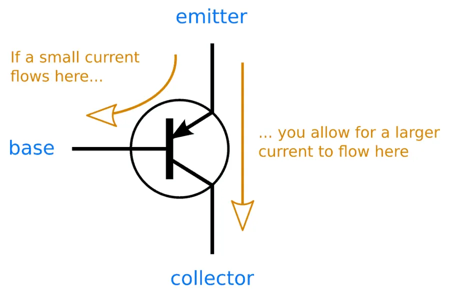
The NPN BJT (Bipolar Junction Transistor) operates by controlling the flow of current between its collector and emitter terminals using a small current applied to its base terminal. This fundamental mechanism enables the transistor to function as both an electronic switch and an amplifier, underpinning its widespread use in electronic circuits.
At its core, an NPN BJT consists of three semiconductor regions: two N-type regions (the collector and emitter) separated by a thin P-type region (the base). The key to understanding its operation lies in how these regions and their respective charge carriers (electrons and holes) interact under different biasing conditions.
When no current flows into the base, the transistor is in a 'cutoff' state, and effectively, no current flows between the collector and the emitter, due to a high resistance barrier at the junctions. However, even a small current flowing into the base can dramatically change this condition.
When a positive voltage is applied to the base relative to the emitter, a small base current (Ib) begins to flow. This current injects electrons from the emitter into the base region. Because the base is extremely thin, most of these electrons are swept into the collector region due to the collector-base voltage, thereby creating a much larger collector current (Ic), proportional to the base current and amplified by a factor called 'current gain' (β or hFE). This phenomenon is the essence of current control in an NPN BJT. This relationship between the base and collector currents is the basis for amplification.
Thus, the NPN transistor's functionality is predicated on the principle of manipulating current flow through the collector-emitter path via a minute current applied to the base. This ability to control a larger current with a smaller one makes the NPN BJT a vital component in electronic circuitry. The amount of collector current is approximately equal to the base current times the current gain (Ic = β * Ib).
NPN BJT transistors can be configured in three primary ways, each offering distinct characteristics and thus being suitable for different applications. These configurations are known as common emitter (CE), common base (CB), and common collector (CC), also sometimes referred to as emitter follower.
| Configuration | Input | Output | Current Gain | Voltage Gain | Input Impedance | Output Impedance | Phase Shift |
|---|---|---|---|---|---|---|---|
| Common Emitter (CE) | Base | Collector | High (β) | High | Medium | Medium | 180° |
| Common Base (CB) | Emitter | Collector | Low (α ≈ 1) | High | Low | High | 0° |
| Common Collector (CC) | Base | Emitter | High (β+1) | Low (≈1) | High | Low | 0° |
Each configuration’s characteristics are explored below:
Understanding the key performance parameters of an NPN BJT transistor is crucial for effective circuit design and analysis. These parameters dictate how the transistor behaves under different operating conditions and directly influence the overall circuit performance. Primary parameters include current gain (β), saturation voltage, and breakdown voltage, which are essential in determining the transistor's suitability for specific applications.
| Parameter | Symbol | Description | Impact on Circuit Design |
|---|---|---|---|
| Current Gain | β (hFE) | Ratio of collector current to base current (IC/IB). It indicates the transistor's ability to amplify current. | High β values mean that small base currents can control large collector currents, useful for amplification but also affects the transistor's input impedance and operating point. |
| Saturation Voltage | VCE(sat) | Collector-emitter voltage when the transistor is in saturation, ideally close to zero. Represents the minimum voltage drop across the transistor when it is fully 'on'. | Low saturation voltage ensures efficient switching by minimizing voltage drop across the transistor, crucial for power efficiency in switching applications. High saturation voltage causes power loss and may affect switching performance |
| Breakdown Voltage | BVCEO, BVCBO, BVEBO | Maximum voltage the transistor can withstand before damage occurs. Different breakdown voltages exist for different terminal combinations: collector-emitter (BVCEO), collector-base (BVCBO), and emitter-base (BVEBO). | Exceeding these voltages can destroy the transistor, making it essential to operate within the breakdown voltage limits in the circuit design. Ensuring the supply voltage and transient voltages are below the breakdown is critical for long term component reliability. |
| Transition Frequency | fT | Frequency at which the common-emitter current gain falls to unity (1), a measure of high-frequency performance of the transistor. | fT limits the maximum frequency of operation for signal amplification, crucial for high-speed communication circuits and signal processing. |
| Input Impedance | Zin | The impedance seen at the input of the transistor, typically when the transistor is configured as a amplifier in common emitter configuration. | The input impedance determines the power transfer from the source to the transistor and is very important to understand when designing the bias for the amplifier to prevent saturation or cutoff bias conditions. |
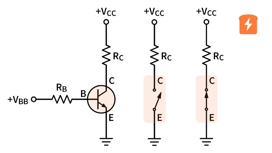
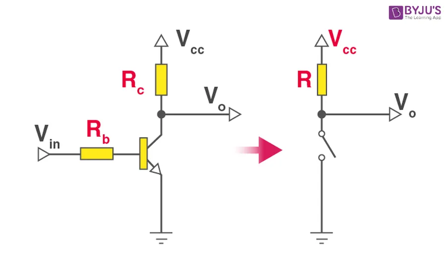
The NPN BJT transistor, when functioning as a switch, leverages its ability to transition between a conductive and non-conductive state, akin to a mechanical switch but with electronic speed and control. This functionality is achieved by modulating the base current, allowing the transistor to operate in distinct regions: saturation, where it behaves as a closed switch, and cutoff, where it acts as an open switch.
The key to understanding this behavior lies in how a small base current can control a much larger collector current.
The transition between cutoff and saturation is extremely rapid, allowing for high-speed switching applications. The actual behavior of the switch is not just on/off, there is a small transition area between the two. The faster the transition, the better, so device designers will try to minimize the amount of time it spends in the active region.
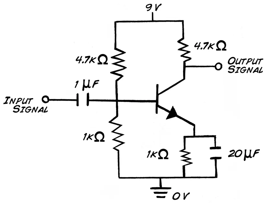
NPN BJT transistors serve as fundamental building blocks for signal amplification in electronic circuits. Their ability to control a larger collector current with a small base current makes them ideal for boosting weak signals to usable levels. This functionality is crucial in various applications, from audio amplifiers to complex communication systems.
The amplification process hinges on the transistor's characteristic of operating in its active region. In this region, a small change in the base current results in a proportionally larger change in the collector current, allowing the transistor to effectively increase the magnitude of an input signal. This gain is quantified by the transistor's current gain (β or hFE) which is the ratio of collector current to base current.
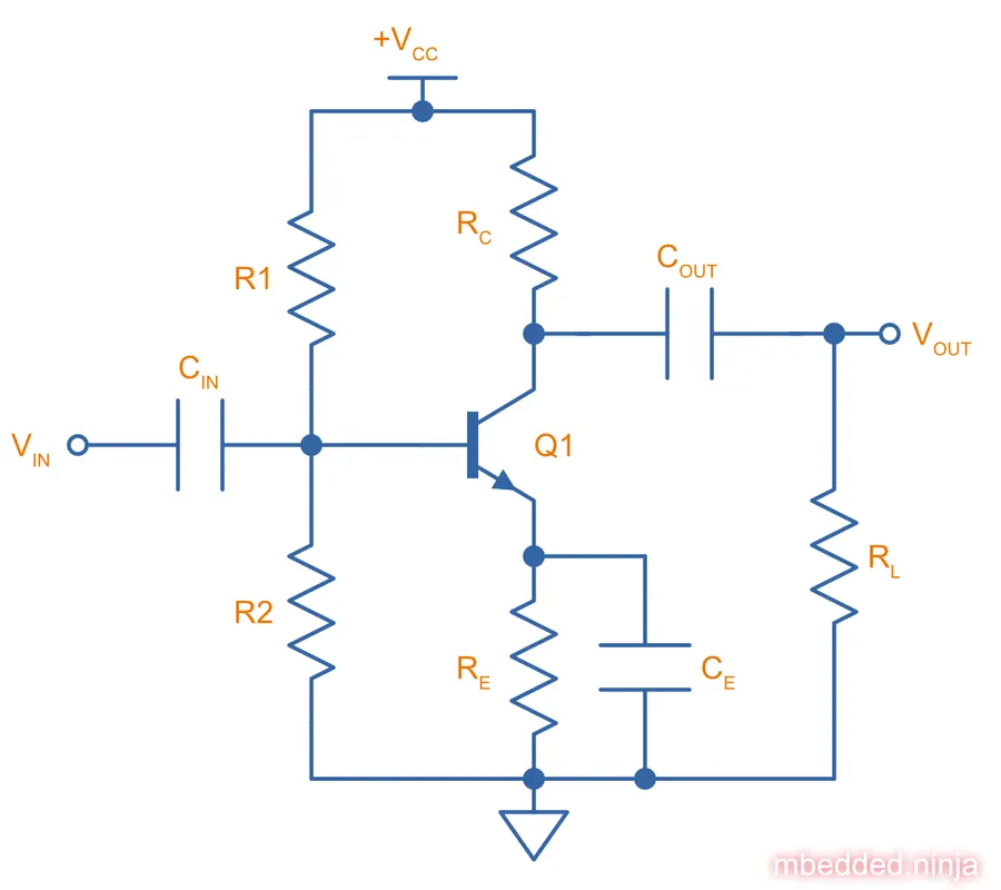
Common amplifier configurations, like the common emitter, exploit this property. In a common emitter amplifier, the input signal is applied to the base, and the amplified output signal is taken from the collector. The transistor amplifies the signal in proportion to its current gain and the external circuit components used for bias and load.
The design and selection of circuit components surrounding the NPN BJT amplifier are carefully selected to achieve the desired gain, bandwidth, and impedance characteristics. Moreover, considerations are made for the input signal level to avoid driving the transistor out of the active region, which can cause signal clipping and distortion.
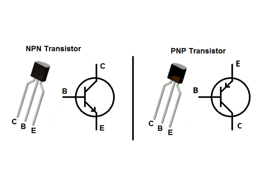
NPN and PNP transistors are the two primary types of bipolar junction transistors (BJTs), distinguished by their doping configurations and resulting current flow characteristics. Understanding these differences is crucial for effective circuit design, allowing engineers to select the appropriate transistor for a specific application.
| Feature | NPN Transistor | PNP Transistor |
|---|---|---|
| Structure | N-type emitter, P-type base, N-type collector | P-type emitter, N-type base, P-type collector |
| Current Flow | Current flows from collector to emitter (electrons) | Current flows from emitter to collector (holes) |
| Polarity of voltages | Positive voltage applied to collector with respect to the emitter to turn it on | Negative voltage applied to collector with respect to the emitter to turn it on |
| Active Region Bias | Base voltage more positive than the emitter | Base voltage more negative than the emitter |
| Switching Behavior | Switches to on state with positive base current | Switches to on state with negative base current |
| Symbol | Arrow on the emitter pointing outwards | Arrow on the emitter pointing inwards |
| Common applications | Low-side switching, current amplification in signal processing | High-side switching, power inverters, and complementary circuit designs |
This section addresses common queries regarding NPN BJT transistors, offering clear and concise answers to enhance understanding of their functionality, characteristics, and applications.
NPN BJT transistors are fundamental building blocks in modern electronics, enabling a vast array of applications due to their ability to switch and amplify electronic signals. Their versatility makes them indispensable in various sectors, ranging from everyday consumer gadgets to complex industrial systems.
In **Consumer Electronics**, NPN BJTs are ubiquitous. For instance, they are used in audio amplifiers within smartphones, headphones, and speakers to boost the signal for clear sound reproduction. They also function as switching elements in power management systems, regulating power delivery to different components.
Within **Automotive Systems**, NPN transistors play a crucial role in the electronic control units (ECUs). These units manage numerous functions including engine timing, fuel injection, and braking systems, relying on the rapid switching capabilities of NPN BJTs. They also are utilized in sensor interfaces for signal conditioning.
In the **Industrial Control** sector, NPN BJTs are integral components of programmable logic controllers (PLCs) and motor drives. PLCs, which control industrial machinery and processes, use NPN transistors as both logic elements and switches for actuators, and in motor control circuitry, NPN BJTs allow precise speed and torque control.
In **Communications**, NPN BJTs are used extensively in radio frequency (RF) amplifiers and mixers within wireless transceivers of devices such as cellular phones. Their low noise characteristics and high gain make them ideal for amplifying weak signals received by antennas.
Consider the example of a simple **LED driver circuit**. An NPN BJT can be configured to act as a switch, turning the LED on and off based on the presence or absence of a base current. This circuit illustrates a basic switching application where a small signal (base current) controls a larger current (collector current) powering the LED. Similarly, in an **audio amplifier circuit**, an NPN BJT will be part of the amplification stage, boosting the input signal to a level suitable for a loudspeaker. The transistor is biased to operate in the linear region of its characteristic curves, enabling signal amplification without significant distortion.
These examples illustrate the versatility and importance of NPN BJT transistors across diverse applications. Their dual functionality as both switches and amplifiers makes them indispensable in a vast array of modern electronic systems, providing the foundation for electronic control and communication.
The NPN BJT transistor, a fundamental building block of modern electronics, is a powerful tool for switching and amplifying signals. Its ability to control large currents with a small input makes it essential in countless applications. Understanding its characteristics and operation allows for its effective use in designing innovative and efficient electronic systems, continuing the advancement of technology in various fields. The exploration of the NPN BJT transistor not only reveals its practical functions but also highlights the elegance of semiconductor physics at work, inspiring further innovation.

