From the ubiquitous smartphone to the sophisticated medical equipment, the PN junction diode stands as a fundamental building block in modern electronics. This unassuming semiconductor device, formed by the union of P-type and N-type materials, allows current to flow in only one direction. In this article, we'll explore the depths of the PN junction diode, uncovering its operating principles, characteristics, and broad range of applications, demonstrating its central role in the evolution of technology.
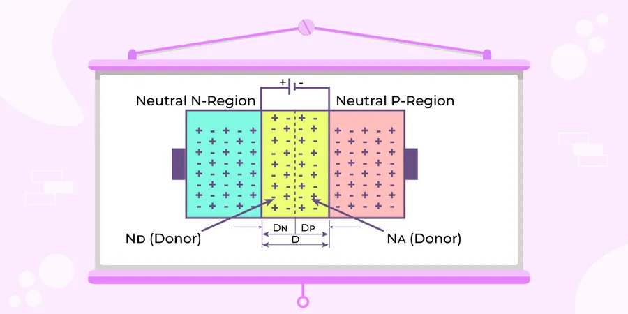
The creation of a PN junction is fundamental to semiconductor device technology, achieved by joining a P-type semiconductor material with an N-type semiconductor material. This process results in a unique electronic structure at the junction interface, enabling the diode's rectifying behavior. The controlled introduction of impurities, known as doping, is crucial to this process.
The formation of a PN junction involves several key aspects:
The critical outcome of this process is the formation of a depletion region and a built-in potential, which is the voltage required to overcome the electric field. These factors are crucial in determining the operational characteristics of the PN junction diode.
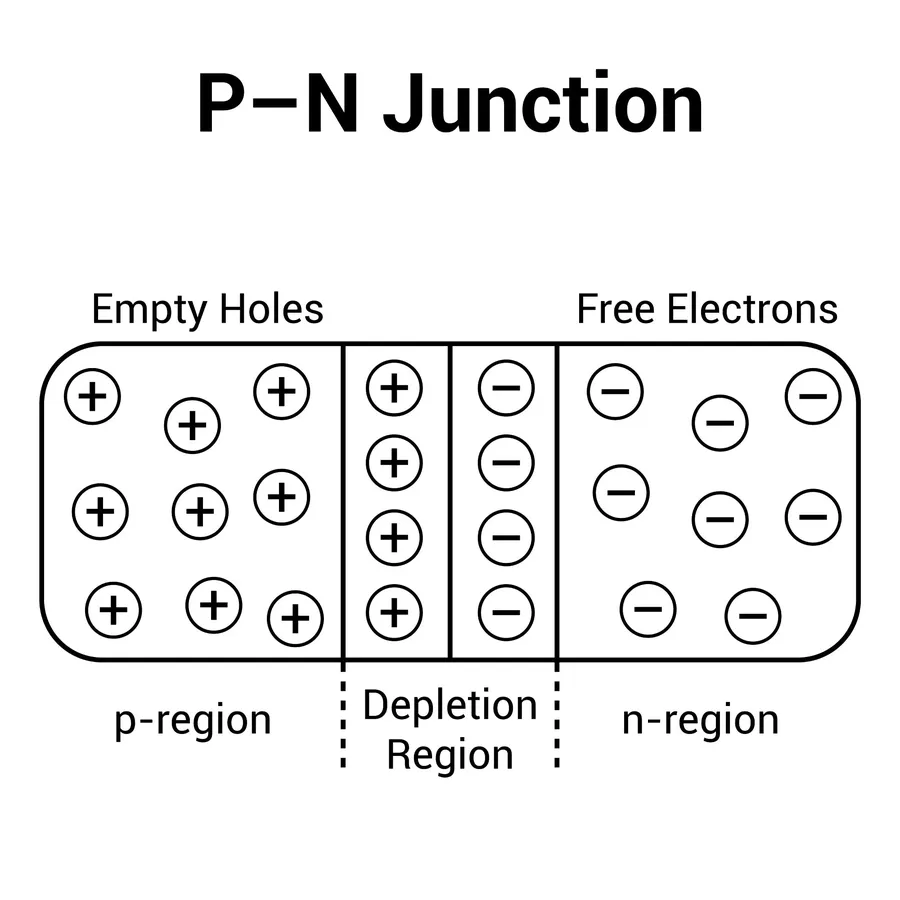
At the heart of a PN junction diode's functionality lies the depletion region and its associated barrier potential. This region forms spontaneously at the interface where P-type and N-type semiconductor materials meet, and the built-in electric field that arises dictates the diode's electrical behavior.
The depletion region, also known as the space charge region, is devoid of mobile charge carriers (electrons and holes). It forms due to the diffusion of electrons from the N-side to the P-side and holes from the P-side to the N-side. This diffusion process leaves behind ionized dopant atoms, which are immobile and create an electric field.
The electric field created by the ionized dopants impedes further diffusion of charge carriers across the junction. This leads to a state of equilibrium where the diffusion current is balanced by the drift current due to the electric field, creating a potential barrier at the junction called built-in potential or barrier potential. The magnitude of the barrier potential depends on the type of semiconductor material and the doping concentration. For silicon, this potential is around 0.7V at room temperature.
| Property | Description |
|---|---|
| Depletion Region | A zone devoid of mobile charge carriers (electrons and holes) that forms at the PN junction interface. |
| Barrier Potential | The built-in potential that opposes the further diffusion of charge carriers across the junction. |
| Formation Mechanism | Diffusion of electrons and holes across the junction, leaving behind immobile ionized dopant atoms. |
The width of the depletion region and the magnitude of the barrier potential are crucial for controlling the flow of current through the PN junction. Applying external voltage will change the width of the depletion region and directly influence the current flow across the junction. Understanding this behaviour is critical to controlling the performance of a PN junction diode.
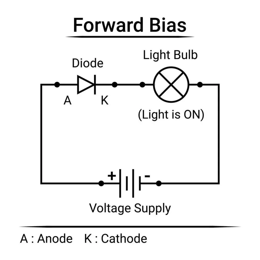
Forward biasing a PN junction diode involves applying an external voltage across the diode in such a way that the positive terminal of the voltage source is connected to the P-type material and the negative terminal is connected to the N-type material. This applied voltage opposes the built-in potential barrier, effectively reducing the width of the depletion region and enabling current flow.
When a forward bias voltage is applied, electrons from the n-side and holes from the p-side are pushed towards the junction, resulting in a decrease in the depletion region width. If the applied voltage exceeds the built-in potential (typically around 0.7V for silicon diodes), the diode will begin conducting current. The current increases exponentially with a small increase in voltage.
The relationship between the applied voltage and the resulting current is described by the diode's current-voltage (I-V) curve. In the forward bias region, the I-V curve shows a characteristic exponential increase in current with increasing voltage. The point where the current starts to increase rapidly is known as the 'knee' voltage, approximately the built-in potential. Beyond this voltage, the diode is considered to be conducting.
Key aspects of forward biasing are:
Understanding forward biasing is crucial to designing and utilizing diodes in circuits where the flow of current in one direction is needed. This behavior forms the basis for numerous applications, including signal rectification and voltage regulation.
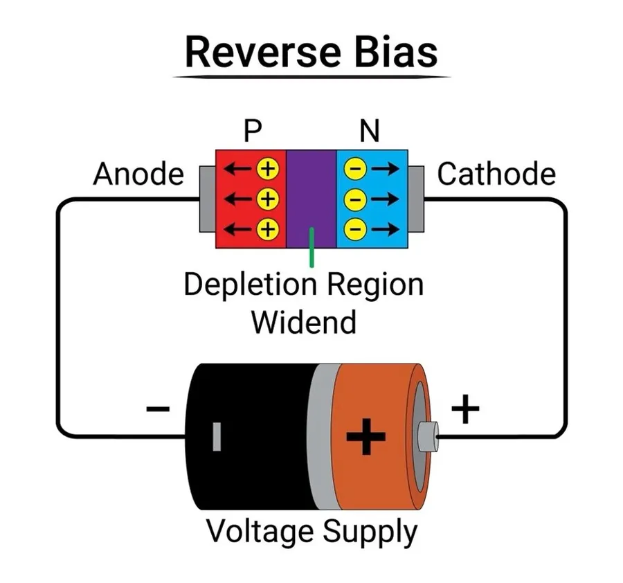
Reverse biasing a PN junction diode involves applying an external voltage source such that the positive terminal is connected to the N-type material and the negative terminal to the P-type material. This configuration significantly alters the behavior of the diode by widening the depletion region and impeding the flow of majority charge carriers.
Under reverse bias, the applied voltage reinforces the built-in potential barrier, causing majority carriers (electrons in the N-type region and holes in the P-type region) to move further away from the junction. This expansion of the depletion region effectively insulates the two sides, dramatically increasing the junction's resistance. Consequently, an ideal diode would allow negligible current flow.
However, in reality, a small current, known as the reverse saturation or leakage current, does flow through the diode. This current is due to the minority carriers (holes in the N-type region and electrons in the P-type region) that are thermally generated within the semiconductor material. The reverse leakage current is significantly smaller than the forward current and is temperature-dependent, increasing as the temperature rises.
Furthermore, as the reverse bias voltage is increased, the depletion region widens further and the electric field strength across the junction increases. If the reverse voltage becomes too high, a phenomenon known as reverse breakdown occurs. During reverse breakdown, the electric field is strong enough to accelerate the minority carriers causing impact ionization, which causes an avalanche of charge carriers. This leads to a sudden and dramatic increase in reverse current, potentially damaging the diode if not limited by an external circuit.
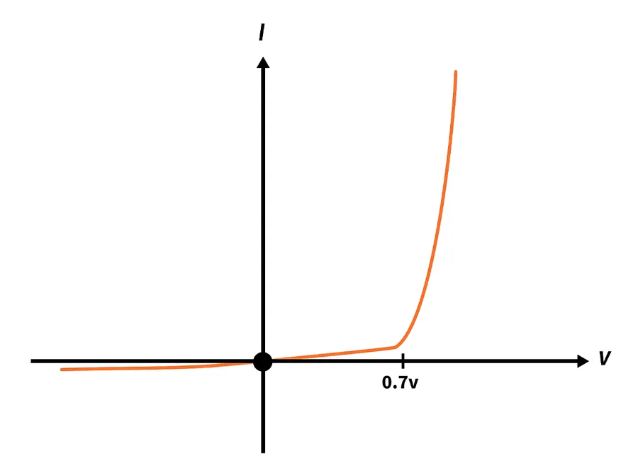
The behavior of a PN junction diode is fundamentally described by its current-voltage (I-V) characteristics, which illustrate how the current through the diode varies with the applied voltage. These characteristics are crucial for understanding diode performance in electronic circuits, revealing key parameters like forward voltage drop, reverse breakdown voltage, and the influence of temperature.
| Characteristic | Description | Typical Value (Silicon Diode) | Effect of Temperature |
|---|---|---|---|
| Forward Voltage Drop (Vf) | The voltage across the diode when it is conducting current in forward bias. | ~0.7 V | Decreases slightly with increasing temperature |
| Reverse Breakdown Voltage (Vbr) | The reverse voltage at which the diode begins to conduct significant reverse current and potentially damage. | Varies widely, from a few volts to thousands, depending on the diode's structure. | Decreases with increasing temperature |
| Reverse Saturation Current (Is) | The small leakage current that flows under reverse bias. | Very small, in the nano-ampere (nA) range. | Increases significantly with increasing temperature |
| Threshold Voltage (Vt) | Minimum forward bias voltage required for the diode to start conducting significantly. Related to the forward voltage drop. | ~0.6 - 0.7 V for silicon. | Decreases with increasing temperature |
| Dynamic Resistance (Rd) | The resistance of the diode in forward bias, calculated as the change in voltage divided by change in current. | Relatively low (typically a few ohms to tens of ohms). | Decreases slightly with increasing temperature |
The I-V curve is not linear; it exhibits an exponential behavior in forward bias. Initially, a small increase in voltage leads to a minimal current. However, once the threshold voltage (around 0.6 to 0.7V for silicon diodes) is surpassed, the current rises rapidly. In reverse bias, the current remains very low until the breakdown voltage is reached, at which point the current increases sharply. Temperature is a significant factor affecting I-V characteristics; higher temperature leads to a lower forward voltage drop, decreased breakdown voltage, and an increase in reverse saturation current.
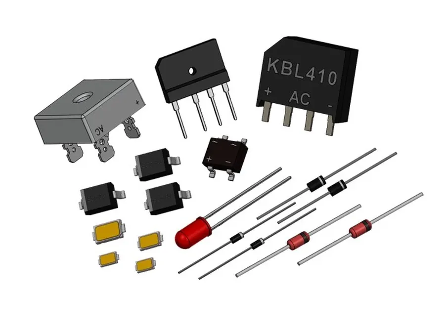
While the fundamental principle of a PN junction remains consistent, its practical implementation leads to a diverse range of diode types, each tailored for specific applications. These variations are achieved through alterations in doping levels, material composition, and structural designs, all built upon the core PN junction concept.
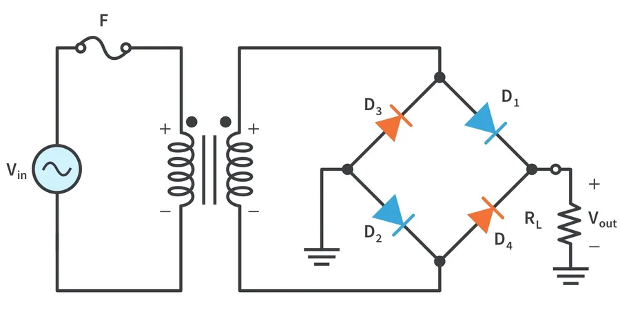
PN junction diodes, fundamental components in modern electronics, exhibit a wide array of applications by exploiting their unique current-voltage characteristics. They serve as essential building blocks in various electronic systems, from power supplies to optoelectronic devices, and even in signal processing.
This section addresses common questions regarding PN junction diodes, offering clear and concise answers to enhance understanding of their fundamental principles and applications.
The versatility of the PN junction diode is evident in its diverse applications, each leveraging its fundamental properties for specific functionalities. This section provides a comparative analysis of the diode's performance across three key applications: rectification, light emission (LEDs), and light detection (photodiodes).
| Application | Principle of Operation | Forward Bias | Reverse Bias | Primary Function | Key Performance Metrics |
|---|---|---|---|---|---|
| Rectifier | Utilizes the diode's unidirectional current flow to convert AC to DC | Low forward voltage drop, high forward current | High reverse blocking voltage, minimal reverse current | AC-to-DC conversion | Efficiency, forward voltage drop, reverse leakage current |
| LED (Light Emitting Diode) | Releases photons at the junction as electrons recombine with holes under forward bias. | Specific forward voltage for light emission, current controls brightness | Non-conductive with minimal reverse bias | Light emission | Luminous intensity, color wavelength, forward voltage |
| Photodiode | Generates current when exposed to light due to the creation of electron-hole pairs at the junction. | Light-induced current increases with light intensity | Reverse bias enhances responsivity, operates in current mode | Light detection and conversion to electrical signal | Responsivity, quantum efficiency, dark current |
The PN junction diode, a seemingly simple device, is the bedrock of modern electronics. Its ability to allow current flow in one direction makes it invaluable in rectifying AC power, generating light, and detecting signals. Understanding the underlying science of the PN junction is essential for comprehending the vast world of semiconductors and their role in our technology-driven world. The continued development and refinement of PN junction diode technologies promise to unlock even greater possibilities for the future of electronics.

