In an increasingly interconnected world, satellite communication stands as a cornerstone for global connectivity, navigation, and Earth observation. At the heart of every robust satellite system lies the signal receiving module, a marvel of miniaturized engineering. Yet, the performance of these critical modules hinges significantly on the underlying Printed Circuit Board (PCB) – a complex interplay of high-frequency signals, sensitive components, and stringent reliability demands. Zero One Solution Limited, a leader in rapid-response PCB assembly solutions since 2011, understands these challenges intrinsically. This article delves into how our specialized PCB solutions are engineered to meet the exacting requirements of satellite signal receiving modules, from design to manufacturing and assembly, empowering innovators to launch their next-generation communication systems with unparalleled efficiency and precision.
The Critical Role of PCBs in Satellite Signal Reception: Ensuring Signal Integrity
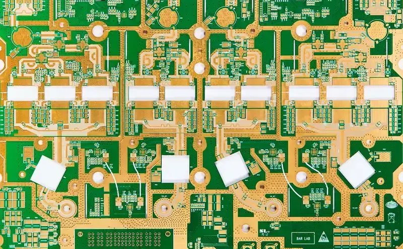
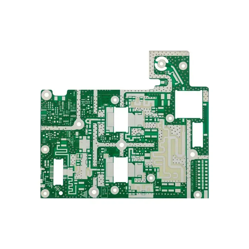
At the heart of every satellite signal receiving module lies the Printed Circuit Board (PCB), a foundational element critical for efficient and reliable signal reception. These PCBs are not merely circuit boards; they are meticulously engineered platforms that ensure the integrity of signals traveling at high frequencies, a necessity for effective communication with satellites. The design and functionality of a PCB directly influence the overall system performance, playing a pivotal role in the success of satellite communication. In the challenging environment of space, where signals are weak and interference is prevalent, the quality of the PCB becomes paramount.
The unique demands of satellite communication necessitate specialized PCB design. These applications operate in high-frequency environments, often involving RF (Radio Frequency) and microwave signals. This necessitates careful consideration of several factors:
Signal Integrity: Maintaining signal integrity is crucial. High-frequency signals are susceptible to attenuation, impedance mismatches, and crosstalk. PCB design must minimize these effects through careful trace routing, impedance control, and selection of appropriate materials.
Noise Reduction: Satellite communication systems are vulnerable to noise from various sources. Effective PCB design incorporates strategies like ground planes, shielding, and filtering to mitigate noise and improve signal-to-noise ratio.
Thermal Management: Operating in extreme temperature environments requires robust thermal management solutions. PCB design must facilitate heat dissipation from sensitive components to ensure operational stability and longevity.
Miniaturization: Space constraints and weight limitations demand miniaturized designs. This often involves advanced manufacturing techniques and the use of compact components, pushing the boundaries of PCB technology.
Addressing these challenges requires expertise in high-frequency PCB design, understanding of RF principles, and access to advanced manufacturing technologies. A well-designed PCB is not just a component; it is the backbone that ensures the successful reception and processing of critical satellite signals, directly impacting the performance and reliability of the entire communication system. For example, a study by the IEEE showed that optimized PCB design can improve signal-to-noise ratio by up to 20% in high-frequency applications. Zero One Solution Limited offers expertise in these specialized areas.
Decoding the Hurdles: Key Challenges in Satellite Signal Receiving Module PCB Design
RF PCB Design Challenges
Designing Printed Circuit Boards (PCBs) for satellite signal receiving modules presents a unique set of challenges that go beyond the realm of standard PCB design. These challenges, rooted in the high-frequency nature of satellite communications and the harsh operating environments, demand specialized expertise and advanced manufacturing capabilities to ensure optimal performance and reliability. Zero One Solution Limited excels in navigating these complexities, offering tailored solutions to overcome these critical hurdles.
High-Frequency Signal Routing and Impedance Matching Satellite signals operate at extremely high frequencies (GHz), necessitating precise signal routing and impedance control. Any mismatch can lead to signal reflections, loss, and performance degradation. Effective PCB design must incorporate controlled impedance traces, careful component placement, and meticulous via design to maintain signal integrity. Zero One Solution Limited utilizes advanced simulation tools and manufacturing processes to achieve optimal impedance matching, ensuring that signals travel efficiently and reliably.
Noise Reduction and Signal Integrity Minimizing noise interference is paramount in satellite signal reception. PCBs must be designed to mitigate both internal and external noise sources. This involves strategic ground plane design, shielding techniques, and the use of appropriate filtering components. Zero One Solution Limited employs advanced noise reduction strategies, including multi-layer PCB designs with optimized ground planes and careful component selection, to ensure clean and clear signal reception.
Thermal Management in Extreme Environments Satellites operate in environments with significant temperature variations, making thermal management crucial for PCB reliability. High-power components generate heat, which, if not dissipated effectively, can lead to performance degradation or failure. Our designs incorporate thermal vias, heat sinks, and advanced materials to ensure optimal heat dissipation, maintaining operational stability across a wide temperature range.
Miniaturization and Component Density Space constraints demand miniaturized designs with high component density. This requires advanced PCB fabrication techniques, including fine-line spacing, blind and buried vias, and sophisticated component placement strategies. Zero One Solution Limited offers expertise in high-density PCB design and manufacturing, enabling compact and powerful satellite signal receiving modules.
Addressing these challenges necessitates a deep understanding of RF engineering, advanced materials, and state-of-the-art manufacturing processes – areas where Zero One Solution Limited excels. Our RF PCB design capabilities, combined with our rapid prototyping services, allow us to create robust and reliable PCB solutions for the demanding requirements of satellite signal reception. Our focus is not only on meeting current technical requirements, but also in enabling the future of satellite technology, one PCB at a time.
Zero One Solution Limited: Your Partner in High-Frequency & RF PCB Excellence for Satellite Applications
High-Frequency PCB Manufacturing Expertise
In the demanding realm of satellite signal reception, the performance of the Printed Circuit Board (PCB) is paramount. Zero One Solution Limited stands as a beacon of expertise, providing specialized design and manufacturing solutions tailored for high-frequency and radio frequency (RF) applications. Our commitment to excellence ensures that every PCB we produce meets the stringent requirements of satellite communication systems, where signal integrity and reliability are non-negotiable.
Our capabilities in this domain are rooted in several key areas:
Advanced Materials We utilize high-performance materials such as Rogers and other low-loss dielectrics, essential for minimizing signal attenuation and ensuring optimal performance at high frequencies. These materials are selected based on their dielectric properties and thermal stability, vital for the harsh environments encountered in satellite applications.
Precision Manufacturing Our state-of-the-art manufacturing processes include advanced etching techniques, precise layer alignment, and rigorous quality control measures. These ensure that every PCB meets the exacting specifications required for RF and high-frequency applications, where even minor deviations can severely impact performance.
Expert Engineering Team Our team of experienced RF and PCB design engineers possesses a deep understanding of the complexities of high-frequency design. They leverage advanced simulation tools and design methodologies to optimize signal paths, manage impedance matching, and mitigate noise – all critical factors for ensuring robust performance in satellite signal receiving modules.
Rapid Prototyping Advantage We excel in rapid prototyping, allowing our clients to quickly iterate and refine their designs. This agility is crucial in the fast-paced satellite industry, where time-to-market and innovation are key competitive advantages. Our rapid prototyping services enable faster design validation and performance testing.
Our expertise extends to various aspects of RF PCB design, including:
Impedance Matching Ensuring precise impedance control is critical for minimizing signal reflections and maximizing power transfer. We design and manufacture PCBs with controlled impedance to meet specific application requirements.
Signal Integrity Analysis We employ advanced simulation tools to analyze signal integrity, identifying and mitigating potential issues such as signal loss, crosstalk, and noise. This ensures that the signal quality is preserved throughout the PCB.
Thermal Management We consider thermal management from the design stage, implementing features such as thermal vias and heat sinks to ensure reliable operation in extreme temperature environments. Effective thermal management is crucial for the longevity and performance of satellite components.
Miniaturization We specialize in designing compact and efficient PCBs, optimizing the use of space while maintaining high performance. Our miniaturization capabilities are particularly valuable for satellite applications where space is at a premium.
Zero One Solution Limited is more than just a PCB manufacturer; we are your strategic partner, dedicated to providing innovative and reliable solutions for the demanding needs of the satellite industry. Partner with us to elevate your satellite signal receiving module designs and achieve unparalleled performance.
Comprehensive One-Stop Services for Satellite Signal Receiving Modules: Design, Manufacturing, and Assembly
Comprehensive PCB Assembly Services
Zero One Solution Limited provides comprehensive one-stop services, streamlining the entire process from initial design to final assembly of Satellite Signal Receiving Module PCBs. Our integrated approach ensures a seamless workflow, dramatically reducing lead times and enhancing project efficiency. By consolidating all aspects of PCB development under one roof, we offer unparalleled control over quality and a significant advantage in today's competitive market.
Our services encompass the following key areas:
PCB Design and Layout Expert design services tailored for high-frequency and RF applications. Our engineers utilize advanced design tools to optimize signal integrity, impedance matching, and minimize noise, crucial for satellite communication systems.
Rapid Prototyping Fast-turnaround prototyping services allow for quick iteration and testing of designs. This capability enables rapid refinement of PCB layouts and performance verification, crucial for accelerating product development cycles.
PCB Manufacturing State-of-the-art manufacturing facilities equipped to handle complex PCB designs, including those with multiple layers, high-density interconnects, and specialized materials like Rogers. We adhere to strict quality control standards throughout the manufacturing process.
Component Sourcing Strategic partnerships with reputable component suppliers ensure reliable access to high-quality components. We manage the component procurement process, reducing the burden on our clients and ensuring timely delivery of all necessary parts.
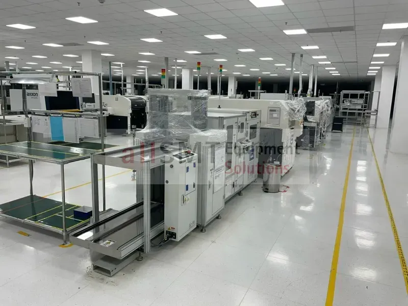
PCB Assembly Professional PCB assembly services, including surface-mount technology (SMT) and through-hole technology (THT) assembly. Our assembly processes are optimized for precision and reliability, essential for the complex requirements of satellite applications.
Testing and Quality Assurance Comprehensive testing and quality assurance measures are implemented at every stage, including electrical testing, functional testing, and environmental testing. This rigorous approach guarantees the performance and reliability of the final product, meeting the stringent demands of the satellite industry.
By choosing Zero One Solution Limited, clients benefit from a single point of contact, eliminating the complexities of managing multiple vendors. This integrated service model not only simplifies the supply chain but also enhances communication, reduces the risk of errors, and ultimately delivers high-performance, reliable PCB solutions for satellite signal receiving modules. Our commitment to excellence ensures that your projects are executed with precision, efficiency, and unwavering quality.
Accelerating Satellite Technology Innovation with Rapid Prototyping
Accelerating Innovation with PCB Rapid Prototyping
In the dynamic realm of satellite technology, the capacity to rapidly prototype and iterate designs is not just advantageous; it's essential. Zero One Solution Limited specializes in providing rapid prototyping services that significantly accelerate the development cycle of satellite signal receiving modules. This approach enables engineers to swiftly refine designs, validate performance metrics, and ultimately, bring innovative solutions to market with unmatched speed and efficiency, thereby offering a substantial competitive edge.
The benefits of rapid prototyping are multifaceted:
Faster Time-to-Market: Rapid prototyping compresses the development timeline, allowing new products and features to reach the market sooner. This is crucial in the rapidly evolving satellite industry where staying ahead of technological advancements is key.
Reduced Development Costs: Early-stage identification and correction of design flaws through iterative prototyping minimize costly rework and reduce overall project expenses. This proactive approach ensures resources are utilized efficiently.
Enhanced Design Optimization: Quick iterations allow for thorough testing and refinement of PCB designs under real-world conditions. This iterative process leads to optimized performance, signal integrity, and reliability of the satellite signal receiving modules.
Increased Innovation: The ability to quickly test and validate new design concepts encourages innovation. This iterative process allows for experimentation with novel technologies and approaches, fostering breakthroughs in satellite communication.
Improved Risk Management: Rapid prototyping allows for risk mitigation by identifying potential issues early in the development cycle. This proactive approach reduces the chances of significant problems arising later in the project, which can be more expensive to fix.
Zero One Solution Limited's rapid prototyping process typically involves the following steps:
Initial Design and Simulation: Our team begins with a comprehensive design phase, followed by simulation to predict performance and identify potential design flaws.
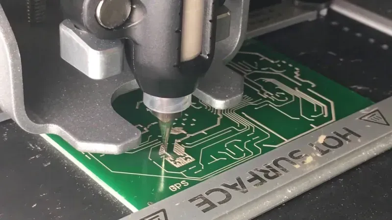
Rapid PCB Fabrication: Using advanced manufacturing techniques, we quickly fabricate the initial PCB prototypes. This allows for minimal lead times, enabling faster iterations.
Component Sourcing and Assembly: We source high-quality components and assemble the prototypes with precision, ensuring that the modules meet all required specifications.
Testing and Validation: Each prototype undergoes rigorous testing and validation to ensure performance meets the required standards. This includes RF testing to evaluate signal integrity.
Iteration and Refinement: Based on the testing results, the design is refined and improved. This iterative process continues until the desired performance is achieved.
By leveraging Zero One Solution Limited's rapid prototyping services, companies can significantly shorten their development cycles, reduce costs, and accelerate the delivery of innovative satellite signal receiving module solutions. Our commitment to speed, precision, and quality makes us the ideal partner for your next satellite technology project.
Ensuring Unwavering Reliability: Quality Assurance in Satellite PCB Manufacturing
Quality Assurance in Satellite PCB Manufacturing
The unforgiving environment of space demands the highest standards of reliability and performance from satellite components, making rigorous quality assurance (QA) an indispensable aspect of PCB manufacturing for satellite signal receiving modules. At Zero One Solution Limited, we understand that the success of your mission depends on the flawless execution of every PCB. Our commitment to uncompromising quality ensures that each board not only meets but exceeds the stringent demands of space applications, offering peace of mind and operational longevity.
Our QA process integrates several key steps:
Material Verification We start with meticulous verification of all incoming materials, including substrates, copper foils, and components, to ensure they meet the required specifications and certifications, such as IPC standards. This step prevents potential defects that might arise from substandard materials.
In-Process Inspection Throughout the manufacturing process, we employ a series of in-process inspections, including Automated Optical Inspection (AOI), to detect any defects early. AOI systems meticulously scan each PCB layer for shorts, opens, and dimensional inaccuracies, enabling immediate corrective actions.
Electrical Testing Every PCB undergoes comprehensive electrical testing, including impedance testing and functional testing, to verify its electrical performance. These tests are essential to ensure that the PCB will perform as designed within the satellite module.
Environmental Testing We simulate the harsh conditions encountered in space, including extreme temperatures, vibrations, and vacuum environments. These tests ensure the PCB can withstand the rigors of launch and the operational environment.
Compliance and Standards Our manufacturing processes are aligned with IPC standards, and we offer certifications to meet specific industry regulations such as those for aerospace. This adherence gives clients the assurance that our products meet the necessary quality requirements for space applications.
By integrating these rigorous QA measures, Zero One Solution Limited ensures that every satellite PCB solution provides the reliability and performance your mission demands. We are committed to being a trusted partner in your success, providing quality and innovation every step of the way.
Frequently Asked Questions About Satellite Signal Receiving Module PCB Solutions
Understanding the intricacies of Satellite Signal Receiving Module PCB Solutions is crucial for both engineers and project managers. This FAQ section addresses common queries to provide clarity on design, manufacturing, assembly, and the specialized services offered by Zero One Solution Limited.
What are the primary challenges in designing PCBs for satellite signal reception? The main challenges include high-frequency signal integrity, impedance matching to minimize signal loss, noise reduction to ensure clear signal reception, thermal management to handle heat generated by components, and miniaturization to fit within size constraints. At Zero One Solution Limited, we specialize in addressing these challenges through advanced materials, precise manufacturing, and expert design practices. For example, we utilize high-frequency laminate materials and controlled impedance routing to maintain signal integrity.
How does Zero One Solution Limited ensure the reliability of PCBs for satellite applications? Zero One Solution Limited employs rigorous quality control measures, including strict adherence to industry standards, comprehensive inspection processes, and environmental testing. We perform thorough electrical testing, functional testing, and environmental stress testing (such as temperature cycling and vibration testing) to guarantee long-term operational stability in harsh space environments. This includes the use of IPC standards and other industry-accepted quality assurance protocols.
What specific RF PCB design capabilities does Zero One Solution Limited offer? Our RF PCB design capabilities include expertise in high-frequency circuit design, RF component integration, impedance control, signal integrity analysis, and RF layout optimization. We support a wide range of RF frequencies and offer services from schematic capture to PCB layout, simulation, and prototyping. We use advanced simulation tools to validate designs before manufacturing and ensure optimal performance of your satellite PCB.
Can Zero One Solution Limited handle both the design and manufacturing of satellite signal receiving module PCBs? Yes, Zero One Solution Limited provides comprehensive one-stop services, covering design, prototyping, manufacturing, component sourcing, and assembly. This integrated approach simplifies the supply chain, reduces lead times, and ensures consistent quality control throughout the entire project lifecycle. Our team works closely with clients from the initial design phase through to final assembly and testing.
How does rapid prototyping benefit the development of satellite signal receiving modules? Rapid prototyping allows for quick iteration and testing of designs, enabling engineers to refine performance, validate functionalities, and bring innovative solutions to market faster. This capability provides a competitive edge, allowing for faster response to emerging market needs and technological advancements. Our rapid prototyping services are designed to accelerate your development cycle, reducing time-to-market.
What materials are used in the manufacture of high-frequency PCBs for satellite applications? We typically use high-frequency laminates such as Rogers and Taconic materials due to their superior dielectric properties, low loss, and excellent signal integrity characteristics. These materials are critical for minimizing signal attenuation and ensuring efficient signal reception in the challenging conditions of space. We also provide material selection guidance to optimize performance based on your specific requirements.
The journey from concept to deployment in satellite communication demands not just innovation, but also robust and reliable hardware. Zero One Solution Limited's expertise in PCB solutions for satellite signal receiving modules offers a clear advantage, combining rapid prototyping capabilities with a deep understanding of high-frequency design and stringent quality control. Our one-stop services, from design to manufacturing and assembly, streamline your development cycle, ensuring that your groundbreaking ideas are transformed into high-performing, market-ready products with exceptional speed and precision. As you navigate the complexities of satellite technology, partner with Zero One Solution Limited to empower your next breakthrough. Contact us today to discuss your specific project requirements and discover how our tailored PCB solutions can accelerate your success in the dynamic world of satellite communication.