Seamless PCB Design & Manufacturing: A Comprehensive Guide
2025.01.05
In today's fast-paced electronics landscape, the synergy between efficient PCB design and reliable PCB manufacturing is crucial. This guide provides a clear understanding of the entire process, explaining the key steps from initial design to final fabrication, empowering both seasoned engineers and hobbyists to navigate the PCB world with confidence.
Understanding the PCB Design Process
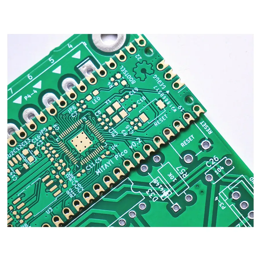
PCB Design Layout
The Printed Circuit Board (PCB) design process is a critical precursor to manufacturing, involving a series of well-defined steps to translate electronic circuit schematics into physical board layouts. This process is paramount to achieving a functional and reliable end-product, and includes schematic capture, board layout, and rigorous design rule checks.
Schematic Capture This initial step involves creating a digital representation of the electronic circuit using specialized software. Symbols representing components are interconnected to establish the electrical relationships as per the design specifications. The quality of the schematic directly impacts the subsequent layout process.
Board Layout The layout phase translates the schematic into a physical board design by placing components and routing electrical traces on the PCB. This step demands careful consideration of component spacing, trace width, layer assignment, and signal integrity to ensure reliable performance and manufacturability.
Design Rule Checks (DRC) Design Rule Checks systematically verify if the physical layout adheres to pre-defined manufacturing constraints and design guidelines. These checks are crucial for identifying errors, preventing potential issues during manufacturing, and ensuring the PCB functions as intended. DRCs encompass aspects like trace spacing, via size, and pad clearances.
Importance of Good Design Practices Employing best design practices throughout the PCB design process is essential for successful manufacturing and long-term reliability. This includes selecting the appropriate materials, optimizing layer stackups, avoiding sharp angles in traces, ensuring proper thermal management, and documenting the design clearly. A well-designed PCB minimizes manufacturing issues and reduces the risk of failures in the final product.
Key Considerations When Choosing a PCB Manufacturer
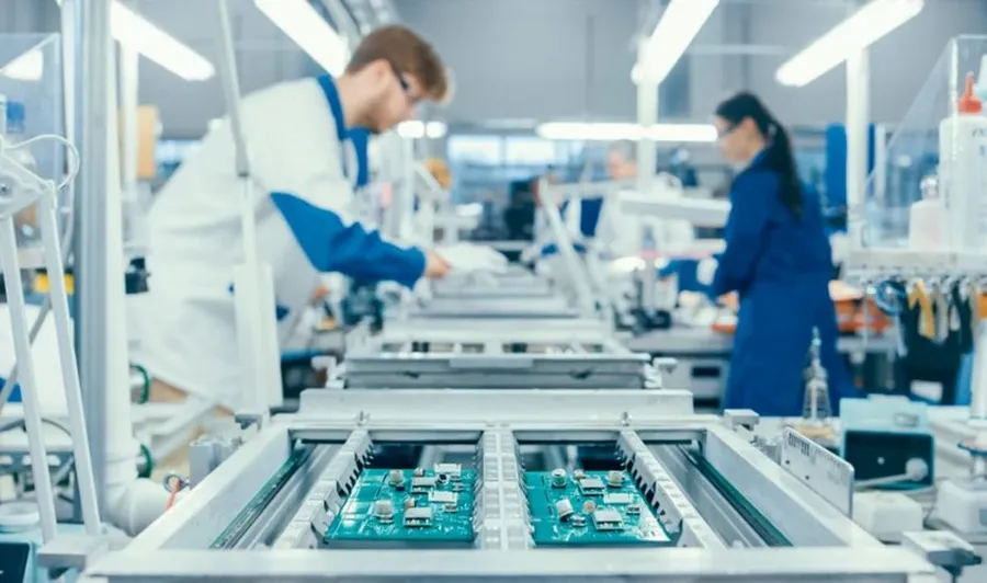
PCB Factory Overview
Selecting the right PCB manufacturer is paramount to the success of any electronics project, impacting not only the final product's quality but also development timelines and overall cost. A thorough evaluation of potential partners involves scrutinizing their production capabilities, material offerings, delivery schedules, and pricing models. Each of these factors plays a critical role, and overlooking any could lead to significant setbacks.
Factor
Description
Impact on Project
Production Capacity
The manufacturer's ability to handle your required volume within your desired timeframe.
Affects project scalability and lead time; inability to meet demand can halt production.
Material Options
Range of substrate materials (e.g., FR-4, Rogers), copper thicknesses, and surface finishes available.
Directly influences performance, durability, and cost of the PCB; limitations can restrict design.
Lead Times
The time required by the manufacturer from order placement to delivery of finished PCBs.
Affects project timeline and time-to-market; excessive delays can result in missed opportunities and increased costs.
Pricing
The cost per board, tooling charges, and any other associated costs of manufacturing.
Directly impacts project budget; balancing cost with quality is essential.
Quality Assurance
The manufacturer's quality control processes, including inspections and testing protocols.
Ensures reliability and consistency of the PCBs; poor quality can result in product failures.
Technology Capabilities
The complexity and sophistication of PCB designs the manufacturer can handle (e.g., number of layers, trace widths, via types).
Limits design possibilities; choosing an incapable manufacturer restricts design scope.
Customer Support
The responsiveness and helpfulness of the manufacturer's support team.
Can affect the efficiency of the design and manufacturing process, especially if issues arise; poor communication can delay projects.
The PCB Manufacturing Process: A Detailed Breakdown
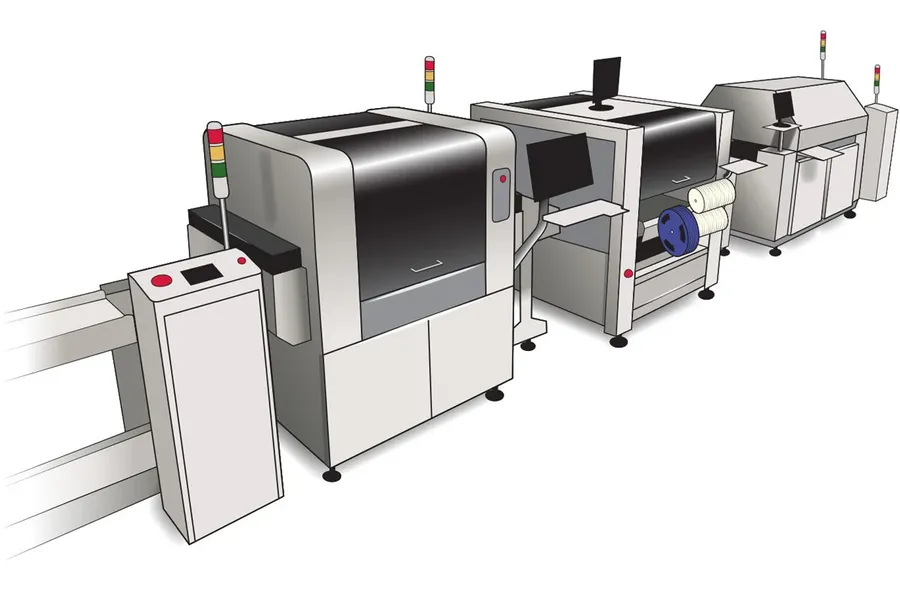
PCB Production Line
The creation of a printed circuit board (PCB) is a meticulous, multi-stage process that transforms a digital design into a physical substrate capable of supporting electronic components. This section provides a comprehensive breakdown of each key step, ensuring a clear understanding of what goes into fabricating a functional PCB.
1. File Preparation and Design Review The process begins with the PCB design files (typically in Gerber format) generated from CAD software. These files are meticulously reviewed to ensure they adhere to manufacturing requirements and design specifications. This initial step is crucial to prevent costly errors later in production.
2. Film Output The Gerber files are used to create photographic films, one for each layer of the PCB. These films act as stencils, transferring the circuit pattern onto the copper-clad laminate.
3. Layer Imaging and Etching The copper-clad laminate is coated with a photosensitive resist. Using the films as a mask, the laminate is exposed to UV light, hardening the resist in the areas that will form the circuit traces. The unhardened resist is then removed, and the exposed copper is etched away in a chemical bath. This leaves the desired copper circuitry.
4. Layer Alignment and Lamination For multilayer PCBs, each etched layer is carefully aligned and then laminated together under high heat and pressure, creating a unified board structure. This process also includes the application of any required insulating layers.
5. Drilling Once laminated, the board undergoes drilling to create the necessary holes for component leads and vias for inter-layer connections. This step is critical for achieving proper electrical connectivity and requires precision machining.
6. Plating and Surface Finish The drilled holes are plated with copper to establish electrical connections between layers. This step is followed by the application of a surface finish, such as HASL, ENIG, or immersion silver, to protect the copper and improve solderability. Surface finish selection is crucial for PCB reliability.
7. Solder Mask and Silkscreen Application A solder mask (typically green) is applied to the board, leaving only the component pads exposed. This prevents solder bridges during assembly. The final step is to apply a silkscreen print (typically white) that labels the components and test points.
8. Final Testing and Inspection Before shipping, each PCB undergoes thorough testing to verify electrical connectivity and functionality, this can include visual inspection and electrical testing of circuit connections. This rigorous quality assurance process ensures each PCB meets the required specifications.
9. Profiling and Packaging Finally the individual PCBs are cut out of the main production panel, this is often achieved through routing or laser cutting, then they are cleaned and carefully packed ready for shipment.
Optimizing PCB Design for Manufacturing (DFM)
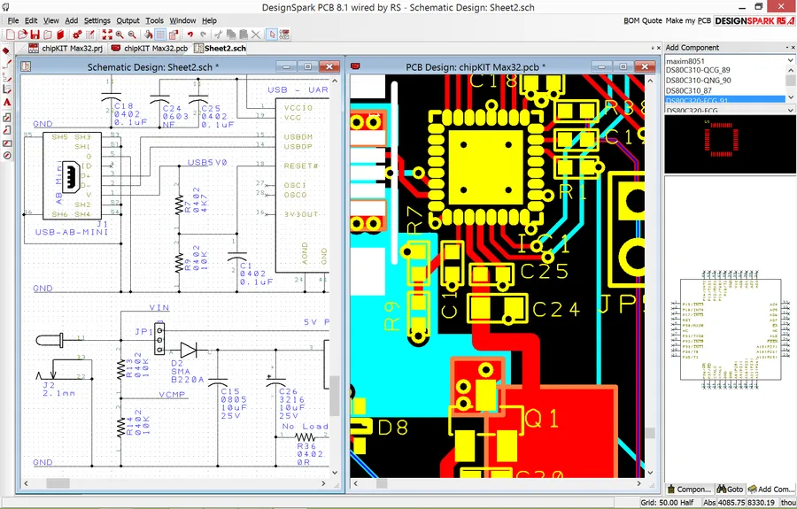
PCB Design Software
Optimizing PCB design for manufacturing (DFM) is paramount to ensure efficient production, reduce costs, and improve the reliability of the final product. DFM involves considering the limitations and capabilities of the manufacturing process during the design phase to avoid potential issues and ensure a smooth transition from design to mass production. This approach minimizes manufacturing errors, reduces rework, and accelerates the time to market for your product.
Component Placement Strategic component placement is crucial. Avoid placing components too close together, particularly near the board edges, to prevent difficulties during assembly. Ensure adequate clearance for soldering and testing probes. Align components with the assembly process to make automated placement more efficient and accurate.
Trace Routing Route traces to prevent signal integrity issues. Avoid sharp 90-degree angles in traces, which can cause impedance mismatches and signal reflections. Utilize wide traces for high-current paths and thinner traces for signal paths. Maintain consistent trace widths to minimize impedance variations.
Via Usage Minimize the use of vias in high-speed signal paths. Vias can cause impedance discontinuities and introduce inductance, which can degrade signal quality. Ensure vias are of an adequate size for proper plating. Place vias strategically to avoid thermal stress during soldering.
Panelization Strategies Effective panelization maximizes the use of manufacturing capacity by arraying multiple boards into a single panel. Include break-away tabs for separating the individual boards after assembly. Consider the efficiency of the assembly line, optimizing panelization to minimize waste and reduce manufacturing costs.
Solder Mask and Stencil Design Ensure adequate solder mask clearance around pads to prevent solder bridging during reflow. Design stencils to accurately deposit solder paste onto pads, optimizing for solder paste volume, and consistent coverage.
Design Rule Checks (DRC) Regularly perform DRC throughout the design process to identify design flaws early. Address errors before sending the design to manufacturing, to reduce the chances of having to modify the design post-manufacturing.
DFM Consideration
Best Practice
Impact
Component Spacing
Maintain sufficient clearance
Prevents assembly issues
Trace Width
Use appropriate widths for current
Reduces signal loss and overheating
Via Placement
Minimize vias in high-speed paths
Maintains signal integrity
Panelization
Efficiently panelize for assembly
Reduces waste and costs
Solder Mask
Adequate clearance
Prevents solder bridging
Rapid Prototyping: Accelerating Your PCB Development
PCB Prototype
Rapid prototyping in PCB development is an essential approach to swiftly validate and refine designs before committing to full-scale production. This iterative process leverages quick-turn manufacturing services, enabling engineers to test design concepts, identify potential flaws, and optimize performance within compressed timeframes and reduced costs. Rapid prototyping allows for physical verification, which is crucial in identifying issues that simulations might miss, leading to more reliable final products.
The core advantages of rapid PCB prototyping can be summarized as follows:
Reduced Time-to-Market Quick-turn services dramatically shorten the design-to-test cycle, enabling faster product launches. This is particularly important in highly competitive markets where speed is a key differentiator.
Cost-Effectiveness By identifying and rectifying design issues early in the process, rapid prototyping prevents costly errors and rework during mass production. This cost-saving benefit is highly valuable for projects with budget constraints.
Design Validation Prototyping provides a physical means to evaluate the performance and functionality of a design, ensuring it meets the intended specifications. This also involves testing mechanical fit, thermal behavior, and overall product integration.
Iterative Design Improvement The rapid feedback loop inherent in prototyping allows for continuous refinement of the design, resulting in a more robust and reliable final product. This process often identifies unexpected performance challenges or opportunities for improvement.
Many PCB manufacturers offer specialized rapid prototyping services that include expedited production timelines. These services often feature options such as:
24-Hour Turnaround Options Some manufacturers provide extremely fast turnaround options, sometimes delivering prototypes within 24 hours. This is ideal for urgent projects or when testing iterations are needed quickly.
Expedited Shipping Coupled with fast production, expedited shipping options ensure that the prototypes are delivered as quickly as possible for testing and feedback.
Specialized Materials and Finishes Rapid prototyping services may offer a limited selection of materials and finishes tailored for quick-turn production, still allowing for a reasonable range of test parameters.
Small Batch Production Capabilities Rapid prototyping is well-suited to small-batch production, which allows for flexible manufacturing of the prototypes, ideal for early-stage testing.
When selecting a manufacturer for rapid PCB prototyping, key considerations should include their production capabilities, the material options available, delivery time commitments, and their pricing structure. It is advantageous to select a manufacturer that provides comprehensive support throughout the prototyping process, from design review to post-delivery support. This level of support ensures that any potential design issues are quickly identified and resolved. Therefore, a comprehensive rapid prototyping strategy is critical to achieving optimized PCB designs and efficient manufacturing processes.
PCB Assembly Services and Options
PCB Assembly Workshop
PCB assembly services encompass a range of techniques for mounting electronic components onto a printed circuit board, transforming a bare board into a functional electronic module. The primary methods include Surface Mount Technology (SMT), Through-Hole Technology (THT), and a combination of both, known as mixed technology assembly. Selecting the appropriate assembly method and service is crucial for achieving the desired functionality, reliability, and cost-effectiveness of the final product.
Assembly Type
Component Mounting
Typical Applications
Pros
Cons
Surface Mount Technology (SMT)
Components are soldered directly to the surface of the PCB.
High density, automated assembly, good electrical performance, lower cost for high volumes.
Requires precision equipment, less robust mechanically, more sensitive to thermal stress.
Through-Hole Technology (THT)
Components have leads that are inserted through holes in the PCB and soldered on the opposite side.
Power electronics, prototypes, rugged applications, connectors.
Strong mechanical connections, suitable for manual assembly, higher tolerance for heat.
Lower component density, higher cost for high volumes, requires more space.
Mixed Technology
Combination of SMT and THT components on the same PCB.
Applications requiring a mix of dense circuitry and robust components, such as industrial controls.
Flexibility to use the best of both technologies, can optimize cost and performance.
More complex assembly process, requires careful planning and execution.
Several options are available within these assembly types, including turnkey services (where the manufacturer handles everything from component sourcing to final assembly) and partial services (where the client may provide some components). Considerations when selecting an assembly service should include volume requirements, complexity of the board, component availability, and the desired lead time.
Cost-Effective PCB Manufacturing Strategies
Optimizing PCB manufacturing costs requires a multi-faceted approach, encompassing material selection, design practices, and strategic choice of manufacturer based on production volume and location. This section will explore these critical areas to ensure the most economical production of your printed circuit boards.
Strategy
Description
Cost Impact
Material Selection
Choosing lower-cost substrates like FR-4 over high-performance materials where appropriate.
Significant savings on material costs, can reduce cost by up to 10-20%.
Design Optimization
Implementing design for manufacturability (DFM) principles, such as minimizing layer count, via usage, and board size.
Reduces manufacturing complexity and rework, leading to cost reductions of 5-15%.
Panelization Strategy
Efficiently arranging multiple PCBs on a single panel to maximize material usage and production efficiency.
Minimizes waste and reduces per-unit production cost by 5-10%.
Component Selection
Choosing standard, readily available components over custom or specialty parts.
Lowers component costs and reduces procurement lead times, cost reduction varies greatly.
Manufacturer Selection
Selecting a manufacturer with pricing that aligns with production volume and requirements; balancing domestic and overseas options.
Cost reduction of 20-50% in overseas manufacture, must consider lead times and communication effectiveness
Volume Commitment
Negotiating favorable pricing with the manufacturer by committing to higher production volumes.
Achieve volume discount pricing reducing cost by 5-20%.
Material selection is one of the key elements affecting cost. While high-performance materials offer advantages, FR-4 remains a cost-effective option for most applications and serves as a good baseline. Further cost savings can be achieved by reducing the number of layers in the PCB, using fewer vias where possible, and optimizing board size to reduce material waste. Design optimization and DFM practices also minimize manufacturing complexity. For example, carefully placing components and routing traces can significantly reduce the need for rework and increase manufacturing yields. Furthermore, considering the PCB panelization strategy maximizes material usage, as multiple PCBs can be produced on a single panel. Finally, choosing the right manufacturer for your project is vital. Domestic manufacturing can provide faster turnaround times and better communication, however, overseas manufacturing often presents significant cost reductions and better rates for higher volumes. Choosing the right balance between location, cost and manufacturer is critical for an effective cost strategy.
Frequently Asked Questions About PCB Manufacturing and Design
This section addresses common questions related to PCB manufacturing and design, covering crucial aspects from material selection to production tolerances and pricing.
What are the standard PCB material options, and how do they affect my design? Common PCB materials include FR-4, which is cost-effective and suitable for most applications, and more specialized materials like Rogers or polyimide for high-frequency or high-temperature environments. Material choice impacts performance, cost, and the manufacturing process. Selecting the right material requires considering operating conditions and design requirements, balancing cost and performance. For example, high-frequency applications necessitate materials with low dielectric constants.
How do tolerances impact the performance and cost of my PCBs? Tighter tolerances in PCB manufacturing, such as trace width, spacing, and hole diameter, increase the cost but can be necessary for high-performance designs. Standard tolerances are generally acceptable for most applications, but precision designs, such as those involving high-frequency circuits or dense component layouts, require tighter control to ensure proper functioning. The specification of tolerances must be based on a detailed understanding of the design’s requirements.
How does PCB design impact manufacturability and cost? Design choices significantly impact manufacturability and cost. Factors such as component placement, trace routing, via usage, and panelization strategy must be optimized for efficient production runs. Poor layout choices can cause manufacturing issues and cost increases. For instance, using standard component footprints and minimizing the number of via sizes can reduce manufacturing complexity and cost.
What factors determine the cost of PCB manufacturing? PCB manufacturing costs are influenced by several factors, including material choice, board size, layer count, feature size, surface finish, order volume, and the manufacturer's capabilities. Complex designs, smaller feature sizes, and special materials will drive up the cost. The cost is usually a function of the complexity and requirements of the design relative to the manufacturer's process capabilities.
What are the key stages in the PCB manufacturing process? The PCB manufacturing process involves several key steps. It begins with file preparation and film output, moves to layer etching, lamination, and drilling, and ends with surface finishing and final testing. This process ensures the proper construction and functionality of the circuit board, as each step is critical to achieving a high-quality finished product. Understanding each step is important in addressing design issues that may cause manufacturing problems.
What is the difference between PCB prototyping and production runs? PCB prototyping involves small production runs of boards to validate designs prior to mass production. Prototyping provides an opportunity to identify and address any design issues before committing to large orders, which can be more costly. It uses the same manufacturing processes but with an emphasis on flexibility and cost reduction by producing a small quantity of boards as a proof of concept and design validation.
What are the common surface finish options and how should I choose? Surface finishes protect copper from oxidation and improve solderability. Common options include HASL (Hot Air Solder Leveling), ENIG (Electroless Nickel Immersion Gold), and OSP (Organic Solderability Preservative). HASL is cost-effective but can have uneven surfaces, while ENIG provides excellent solderability and is suitable for fine-pitch components, but at a higher cost. The choice depends on the application requirements and cost constraints. For example, ENIG is ideal for applications requiring high reliability and finer pitches.
Future Trends in PCB Technology
The printed circuit board (PCB) industry is undergoing rapid evolution, driven by advancements in materials science, miniaturization techniques, and the increasing demand for higher performance and more versatile electronic devices. These trends are reshaping PCB design and manufacturing workflows, demanding more sophisticated approaches.
Advanced Materials The future will see the increased use of novel materials with improved electrical, thermal, and mechanical properties. This includes low-loss dielectrics for high-speed applications, thermally conductive materials for better heat dissipation, and flexible substrates for conformal electronics.
Miniaturization and High-Density Interconnects (HDI) The trend towards smaller, more compact electronic devices necessitates higher circuit densities. HDI technology, involving microvias, fine lines, and multilayer structures, will be critical in achieving greater functionality in smaller form factors.
Flexible and Stretchable PCBs Flexible PCBs will enable more innovative designs and applications, particularly in wearable electronics, medical devices, and automotive systems. Stretchable PCBs, representing a more advanced iteration, will further enhance the capabilities of these applications.
Embedded Components Embedding passive components and integrated circuits directly into the PCB substrate offers further gains in miniaturization and improved electrical performance. This technique reduces the overall footprint of electronic assemblies and improves reliability.
Additive Manufacturing (3D Printing) for PCBs Additive manufacturing techniques are revolutionizing PCB fabrication by enabling rapid prototyping, complex 3D designs, and custom solutions. This technology holds the potential to significantly reduce lead times and costs for specialized applications.
Eco-Friendly and Sustainable Practices There is growing emphasis on sustainable practices in PCB manufacturing, including the use of eco-friendly materials and processes, and recycling and recovery of precious metals. This will reduce the environmental footprint of the electronics industry.
Successfully navigating the PCB manufacturing process requires a deep understanding of both PCB design and fabrication. By leveraging the right design practices and partnering with the appropriate PCB manufacturer, you can ensure that your electronic products are both innovative and efficiently produced. Keep exploring to find the latest innovations in the field to enhance your next PCB project from design to manufacturing.