In the vast expanse of the open sea, ship navigation radar stands as a critical technology, ensuring safe passage and collision avoidance. At the heart of this technology lies the Printed Circuit Board (PCB), a silent workhorse responsible for processing and transmitting vital radar signals. Zero One Solution Limited, with its decade-long expertise in PCB solutions and rapid prototyping, recognizes the paramount importance of reliable and high-performance PCBs in marine radar systems. We understand that the quality of the PCB directly impacts the accuracy and dependability of the radar, influencing the safety of vessels and their crew. This article delves into the intricacies of PCB solutions for ship navigation radar, exploring the design considerations, materials, manufacturing processes, and testing procedures that Zero One Solution Limited employs to deliver cutting-edge solutions for this demanding application.
Ship navigation radar systems are the eyes of a vessel at sea, providing critical information for safe passage, collision avoidance, and situational awareness. At the heart of these indispensable systems lie Printed Circuit Boards (PCBs), serving as the backbone for the complex electronic circuitry that processes radar signals. The integrity and performance of these PCBs directly dictate the reliability and accuracy of the entire radar system, making their design and manufacturing a paramount concern in maritime technology.
Modern ship navigation radar systems utilize electromagnetic waves to detect objects and map the surrounding environment, offering vital data regardless of visibility conditions. From large commercial vessels to naval ships and even recreational boats, radar is a non-negotiable navigational aid. The sophistication of these systems, including pulse compression, Doppler processing, and advanced signal filtering, relies heavily on high-performance PCBs capable of handling high-frequency signals with exceptional precision and reliability. Without robust and meticulously engineered PCBs, the intricate functionalities of a radar system would simply not be achievable, highlighting their foundational role in ensuring maritime safety and efficiency.
Designing Printed Circuit Boards (PCBs) for ship navigation radar systems presents a unique set of engineering challenges that demand meticulous attention to high-frequency signal management, precise impedance control, and robust thermal dissipation. These considerations are paramount to ensuring the radar's operational accuracy, reliability, and longevity in the demanding marine environment. Adhering to stringent industry standards and regulatory requirements is not merely a best practice but a critical mandate for safety and performance in maritime applications.
| Design Consideration | Impact on Radar Performance | Key Solution/Approach |
|---|---|---|
| Thermal Management | Prevents component failure, maintains stable operating parameters. | Utilize thermal vias, heat sinks, specialized substrates (e.g., metal core PCBs), and strategic component placement to dissipate heat efficiently. Simulation tools are essential for identifying hot spots. |
| Environmental Resilience | Ensures continuous operation despite harsh marine conditions (corrosion, vibration, humidity, temperature extremes). | Employ robust PCB materials (e.g., high Tg, low moisture absorption), conformal coatings, hermetic sealing, and vibration-resistant component mounting techniques. Compliance with marine-specific standards (e.g., IEC 60945) is critical. |

Selecting the appropriate PCB materials is paramount for ship navigation radar systems, which operate in some of the most challenging environments on Earth. These materials must withstand constant exposure to saltwater, extreme humidity, fluctuating temperatures, and mechanical stress, all while maintaining superior dielectric properties and long-term reliability for critical signal integrity. The right material choice directly impacts the radar's performance, longevity, and ultimately, the safety of maritime operations.
| Material Type | Key Properties | Benefits for Marine Radar PCBs | Considerations |
|---|---|---|---|
| FR-4 (High-Tg) | Good mechanical strength, high glass transition temperature | Improved thermal stability, cost-effective for less demanding sections | Limited high-frequency performance, moisture absorption |
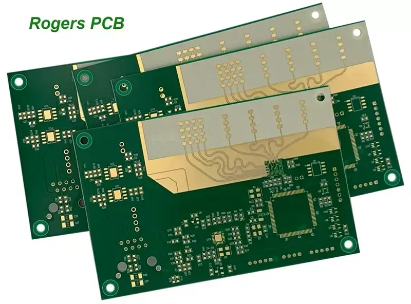
| Rogers/PTFE-based laminates | Excellent dielectric constant stability, low dissipation factor, low moisture absorption | Superior high-frequency performance, stable across temperature and humidity, ideal for RF front-ends | Higher cost, specific processing requirements |
| Polyimide | High temperature resistance, excellent chemical resistance, good flexibility (for flex/rigid-flex) | Reliability in extreme temperatures, robust against corrosive elements | Higher cost, can be more brittle than other high-performance materials |
| Ceramic/Hybrid Substrates | Exceptional thermal conductivity, very low dielectric loss, high stability | Extreme temperature and vibration resistance, highly stable electrical performance | Very high cost, complex processing, limited large-scale application |

Achieving peak performance in ship navigation radar systems hinges critically on the precision and sophistication of their underlying Printed Circuit Boards (PCBs). High-frequency radar applications demand manufacturing techniques that go beyond conventional methods, ensuring signal integrity, minimal loss, and optimal operational stability in demanding marine environments. These advanced processes are vital for fabricating PCBs capable of handling the precise signal transmission and reception required for accurate navigation and collision avoidance.
| Technique | Description | Advantage for Radar PCBs |
|---|---|---|
| Precision Etching | Utilizes highly controlled chemical processes to create extremely fine traces and precise circuit patterns, critical for high-density interconnections. | Enables tighter component spacing and superior signal routing, minimizing interference and signal degradation at high frequencies. |
void setup() {
  // Initialize high-frequency module
  RFModule.begin(10000000000); // Example: 10 GHz operation
  // Configure impedance matching network
  ImpedanceMatcher.setTargetImpedance(50); // Standard 50 Ohm
}

void loop() {
  // Process radar signals
  SensorData = RFModule.read();
  // Apply signal processing algorithms
  ProcessedData = RadarProcessor.process(SensorData);
  // Transmit processed data
  DisplayUnit.send(ProcessedData);
}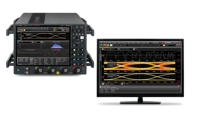
In the high-stakes environment of maritime navigation, the precision and reliability of radar systems are paramount. At the core of this reliability lies impeccable signal integrity and precise impedance control within the Printed Circuit Boards (PCBs). These two factors are critical for minimizing signal loss, preventing electromagnetic interference (EMI), and ensuring accurate, real-time data transmission, which directly impacts the operational effectiveness and safety of a vessel.
| Problem | Impact on Radar Performance | Mitigation Technique |
|---|---|---|
| Signal Reflections | Distorted radar echoes, ghost targets | Impedance matching, proper termination resistors |
| Crosstalk | False positives, reduced signal-to-noise ratio | Adequate trace spacing, differential pairs |
| Ground Bounce | Logic errors, increased EMI | Solid ground planes, multiple ground vias |
| Attenuation/Loss | Reduced radar range and sensitivity | Low-loss dielectric materials, wider traces |
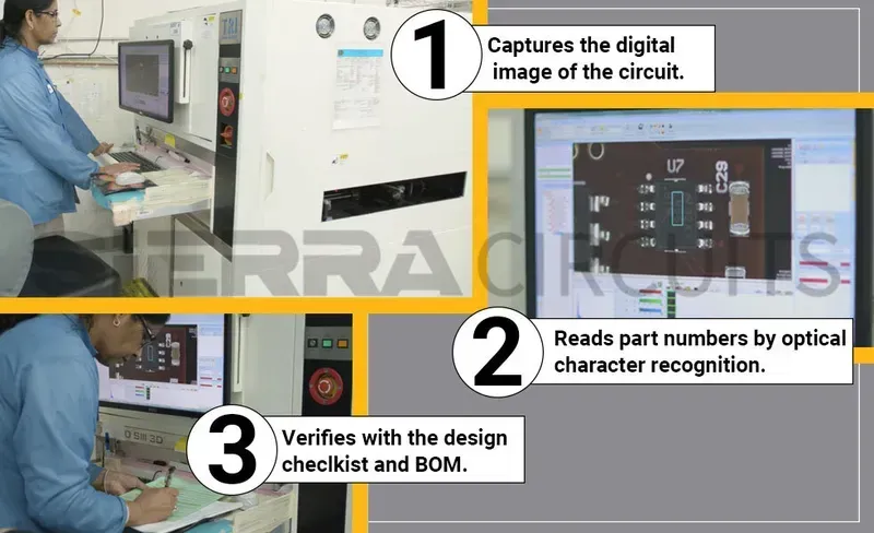
Ensuring the unwavering reliability of ship navigation radar systems hinges critically on meticulous PCB assembly and rigorous testing. Given the demanding marine environment, these processes are not merely manufacturing steps but rather a comprehensive validation of the board's integrity, signal fidelity, and long-term operational resilience. It's about transforming a meticulously designed board into a robust, high-performance module capable of delivering precise navigation data under the most challenging conditions.
| Testing Phase | Purpose | Key Methods |
|---|---|---|
| Functional Testing | Verifies the PCB's electrical performance and validates if it meets design specifications under operational conditions. | In-circuit testing (ICT), Boundary Scan testing, custom functional test fixtures simulating radar signal paths, RF performance measurements (e.g., S-parameters, noise figure). |
| Environmental Stress Screening (ESS) | Exposes PCBs to simulated harsh marine conditions to accelerate potential latent defects and ensure long-term reliability. | Thermal cycling (extreme hot/cold), humidity testing, vibration testing, salt spray testing (for final assembled units or coated PCBs). |
| Burn-in Testing | Operates the PCB under elevated stress conditions (temperature, voltage) for an extended period to identify early-life failures. | Continuous operation at maximum specified temperature and voltage, often with cycling on/off or varied load conditions, for 24-72 hours. |
Each stage of assembly and testing for marine radar PCBs is critical, contributing to the overall integrity and performance of the final navigation system. From precise component mounting to rigorous environmental validation, these processes ensure that Zero One Solution Limited delivers PCBs that meet the stringent demands of maritime applications, guaranteeing reliability and safety at sea.
Zero One Solution Limited stands as a premier partner for ship navigation radar PCB solutions, leveraging over a decade of specialized experience to deliver unparalleled reliability and performance. Our deep understanding of the unique demands of marine environments, coupled with a rapid-response R&D prototype manufacturing capability, positions us as the ideal choice for developers seeking to accelerate their product cycles. We offer a holistic, one-stop service that encompasses every critical phase of PCB development for radar systems, from intricate design and advanced manufacturing to precision assembly and rigorous testing.
With our headquarters in Shenzhen and a branch office in Dubai, Zero One Solution Limited strategically operates within a global PCBA supply chain network. This extensive network provides seamless access to worldwide resources, ensuring efficient procurement of high-quality components and materials, and facilitating rapid turnaround times for even the most complex ship navigation radar PCB projects. Our commitment to rapid prototyping empowers clients to swiftly validate designs and bring innovative solutions to market with exceptional efficiency, reinforcing our position as a leader in specialized PCB solutions for critical maritime applications.
Zero One Solution Limited's unwavering commitment to precision engineering and rapid prototyping has culminated in numerous successful PCB projects for ship navigation radar systems. These case studies underscore our capability to navigate the most complex design challenges and deliver high-performance, resilient solutions that meet the rigorous demands of the maritime industry, solidifying our position as a trusted partner in critical marine electronics.
| Project Name | Challenge | Zero One Solution | Outcome | Key Technologies |
|---|---|---|---|---|
| High-Frequency X-Band Radar Front-End PCB | Ensuring signal integrity at 9 GHz in a compact space with extreme temperature variations. | Utilized advanced RF PCB materials (Rogers 4350B), multi-layer stack-up optimization, and precision impedance control techniques. Employed selective gold plating for superior conductivity and corrosion resistance. | Delivered a highly stable and efficient radar front-end, reducing signal loss by 15% and improving detection range by 10% compared to previous designs. The solution withstood rigorous thermal cycling tests. | RF/Microwave Design, Controlled Impedance, Material Selection (Rogers), Thermal Management |
| Marine S-Band Radar Power Amplifier Module | Designing a high-power PCB capable of dissipating significant heat while maintaining signal stability in a salt-spray environment. | Implemented thick copper layers (3oz) for enhanced thermal dissipation and current handling. Incorporated integrated heat sinks and utilized a specialized conformal coating for environmental protection. | Achieved a 20% improvement in power amplifier efficiency and a 30% reduction in operating temperature, significantly extending the module's lifespan. The coating passed 1000-hour salt spray tests. | High Current/Power PCB Design, Thermal Dissipation, Conformal Coating, Environmental Sealing |
| Integrated AIS Transponder & Radar Display PCB | Miniaturizing a complex digital and analog PCB for combined AIS and radar display functionality with EMI shielding in a confined navigational console. | Employed high-density interconnect (HDI) technology with micro-vias for compact routing. Designed custom EMI shielding layers and optimized ground planes to minimize interference between digital and analog sections. | Successfully integrated multiple functionalities onto a single, compact PCB, reducing the overall product footprint by 25% and enhancing system reliability by mitigating electromagnetic interference. | HDI Technology, EMI/EMC Design, Mixed-Signal Routing, Miniaturization |
| Solid-State Phased Array Radar Antenna PCB | Developing a large-format, multi-layer PCB for a solid-state phased array antenna requiring precise phase control and power distribution across hundreds of elements. | Utilized advanced panelization techniques for large board manufacturing and employed specialized lamination processes for layer registration accuracy. Implemented precision laser drilling for critical through-holes and blind vias. | Enabled highly accurate beam steering and rapid target acquisition for next-generation radar systems. The PCB's robust construction ensured long-term operational integrity in dynamic marine conditions. | Large Format PCB, Phased Array Optimization, Precision Drilling, Power Distribution Networks |
Understanding the intricacies of Printed Circuit Boards (PCBs) for ship navigation radar systems is crucial for ensuring maritime safety and operational efficiency. This section addresses frequently asked questions, providing clear and authoritative insights into the design, manufacturing, and application of these specialized PCBs, directly addressing common concerns and technical considerations in the field of Ship Navigation Radar PCB Solutions.
In conclusion, the PCB is a critical component in ship navigation radar systems, demanding precision, reliability, and adherence to stringent quality standards. Zero One Solution Limited is dedicated to providing advanced PCB solutions tailored to the unique requirements of marine radar applications. From initial design to final assembly, our expertise and commitment to excellence ensure that our clients receive high-performance PCBs that contribute to the safety and efficiency of maritime navigation. Contact Zero One Solution today to discuss your ship navigation radar PCB needs and discover how our solutions can elevate your radar system's performance. Partner with us to navigate the future of maritime technology with confidence.

