In the high-stakes arena of modern naval warfare, electronic warfare (EW) stands as a critical component, dictating dominance through electromagnetic spectrum control. At the heart of these sophisticated EW systems lies the Printed Circuit Board (PCB), the unsung hero responsible for integrating complex electronic components. Zero One Solution Limited recognizes the pivotal role of reliable and high-performance PCBs in shipborne EW systems. With our extensive experience in rapid prototyping, PCB design, manufacturing, and assembly, we are uniquely positioned to deliver cutting-edge PCB solutions that meet the rigorous demands of maritime defense. This article delves into the intricacies of shipborne electronic warfare PCB solutions, highlighting the challenges, design considerations, and the comprehensive services offered by Zero One Solution Limited to ensure mission success.
Introduction to Shipborne Electronic Warfare
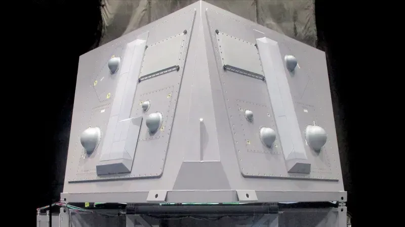
Shipborne electronic warfare (EW) is a critical component of modern naval operations, providing essential capabilities for detecting, intercepting, and disrupting adversarial electromagnetic activities. At its core, shipborne EW aims to gain an information advantage in the electromagnetic spectrum, enabling naval forces to protect assets, ensure safe navigation, and achieve mission objectives in increasingly complex and contested maritime environments. The sophisticated nature of these systems necessitates exceptionally reliable and high-performance Printed Circuit Board (PCB) solutions, which serve as the foundational backbone for all electronic functionalities, from signal processing to power management.
What is Shipborne Electronic Warfare? Shipborne electronic warfare encompasses a broad range of military actions that exploit the electromagnetic spectrum to deny or degrade an adversary's use of it, while ensuring friendly forces can utilize it effectively. This includes electronic support (ES) for intelligence gathering, electronic attack (EA) for disruption, and electronic protection (EP) for self-defense.
Why is EW Crucial for Modern Naval Operations? In contemporary naval engagements, information dominance is paramount. EW systems provide real-time situational awareness, allowing ships to detect and classify threats, jam enemy communications and radar, and protect against missile attacks. Without robust EW capabilities, naval assets are significantly more vulnerable to sophisticated electronic threats.
What Types of Threats Do Shipborne EW Systems Counter? Shipborne EW systems are designed to counter a wide array of threats, including radar-guided missiles, surveillance radars, communication intercepts, and electronic intelligence (ELINT) gathering. They protect against both active and passive threats across various frequency bands.
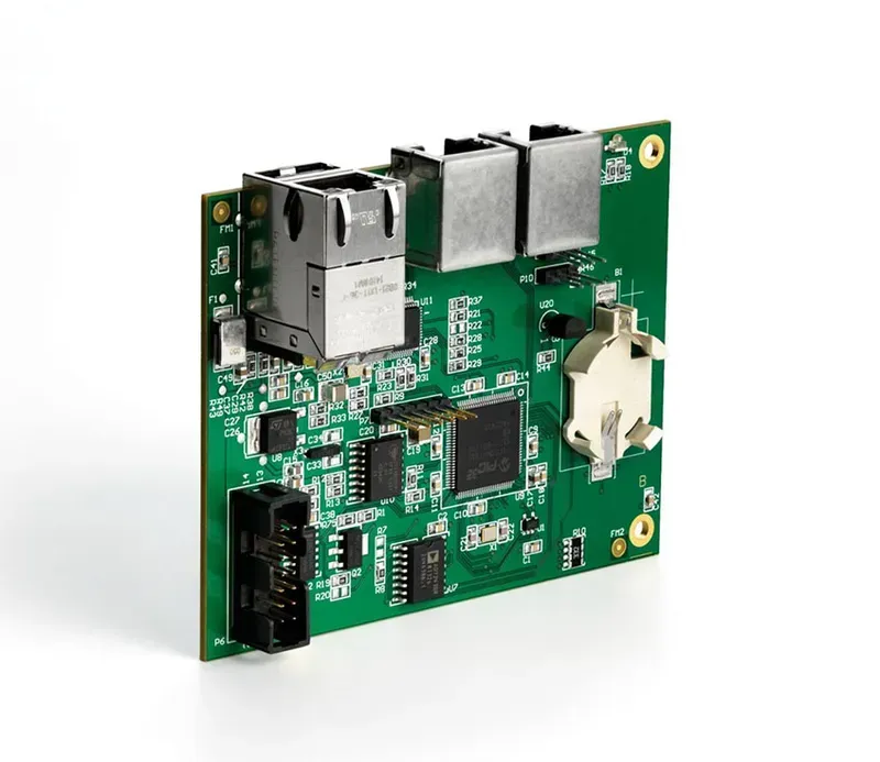
What is the Role of PCBs in Shipborne EW Systems? PCBs are the indispensable foundation of shipborne EW systems, integrating complex components and circuitry that handle high-speed data, RF signals, and power delivery. Their design directly impacts system performance, reliability, and resilience against the harsh maritime environment, making their selection and manufacturing critical for mission success.
How Do Environmental Factors Impact Shipborne EW PCBs? Shipborne EW PCBs operate in extremely challenging environments characterized by constant vibration, sudden shocks, extreme temperature fluctuations, high humidity, and corrosive salt spray. These conditions demand specialized materials, robust design methodologies, and stringent manufacturing processes to ensure long-term operational integrity and reliability.
Challenges in Designing PCBs for Shipborne EW Systems
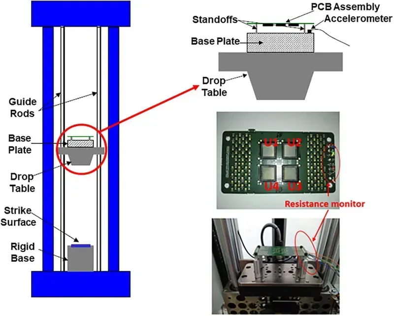
Shipborne PCB Shock Test
Designing Printed Circuit Boards (PCBs) for shipborne Electronic Warfare (EW) systems presents unique and formidable challenges due to the extreme operational environment. Unlike terrestrial or airborne applications, naval platforms are constantly subjected to a trifecta of environmental stressors: relentless shock and vibration, extreme temperature fluctuations, and the pervasive threat of electromagnetic interference (EMI) and corrosive elements. These conditions demand not just robust materials but also sophisticated design methodologies to ensure the unwavering reliability and performance essential for mission-critical electronic warfare capabilities. The core objective is to engineer PCBs that can sustain operational integrity under duress, safeguarding national security assets against evolving electronic threats.
How do shock and vibration impact shipborne EW PCB reliability? Shipborne EW PCBs are exposed to continuous mechanical stresses from engine vibrations, wave impacts, and potential combat scenarios. This leads to fatigue failure in solder joints, component leads, and even the PCB substrate itself. Mitigation strategies include using thicker copper layers, robust component mounting techniques (e.g., underfill, staking), vibration-dampening materials, and optimizing board layout to distribute stress evenly. Adherence to military standards like MIL-STD-810G for shock and vibration testing is crucial to validate design integrity.
What thermal management challenges exist for EW PCBs in a marine environment? Maritime environments subject PCBs to wide temperature swings, from freezing arctic waters to scorching desert seas, coupled with significant heat generation from high-power EW components. Inadequate thermal management can lead to component overheating, performance degradation, and reduced lifespan. Effective solutions include integrating heat sinks, employing thermal vias, utilizing low-thermal-resistance substrates (e.g., ceramics, metal-core PCBs), and incorporating sophisticated active cooling systems, all while considering the space and weight constraints inherent to shipboard integration.
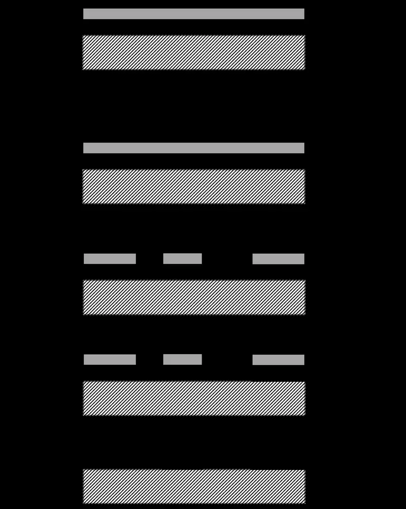
How is electromagnetic interference (EMI) mitigated in shipborne EW PCB designs? Shipborne EW systems operate in an electromagnetically dense environment, requiring precise signal integrity amidst potential interference from ship's own systems (e.g., radar, communication systems) and external threats. EMI can cause signal corruption and system malfunction. Mitigation involves meticulous PCB stack-up design, proper grounding techniques (e.g., dedicated ground planes, multiple ground vias), shielding of sensitive traces and components, careful routing to minimize crosstalk, and the use of EMI filters. Compliance with MIL-STD-461 for electromagnetic compatibility (EMC) is a non-negotiable requirement.
What are the primary concerns regarding corrosion resistance for shipborne EW PCBs? The marine atmosphere, laden with salt spray and high humidity, is highly corrosive. This can degrade solder joints, expose copper traces, and lead to electrical shorts or open circuits, severely impacting PCB functionality. To counter this, material selection is critical, favoring gold-plated finishes, specific solder alloys, and robust conformal coatings (e.g., acrylic, epoxy, silicone) that provide a protective barrier. Hermetic sealing and specialized enclosures are also employed to isolate the PCBs from direct environmental exposure.
Why is reliability paramount for Shipborne Electronic Warfare PCB Solutions? Reliability is non-negotiable in shipborne EW systems because they are critical for national defense, operating in highly dynamic and often hostile environments. Failure of an EW system can have catastrophic consequences, compromising mission success and personnel safety. Therefore, every aspect of the PCB—from material selection and design to manufacturing and testing—must prioritize fault tolerance, longevity, and consistent performance under extreme conditions, ensuring the system functions flawlessly when most needed.
Key Design Considerations for EW PCBs
Designing Printed Circuit Boards (PCBs) for Electronic Warfare (EW) systems, especially those deployed in shipborne environments, necessitates a meticulous approach to several critical considerations. The paramount goal is to ensure unparalleled signal integrity, efficient power distribution, robust thermal management, and judicious component selection. These elements are interdependent and collectively determine the system's ability to operate with precision, minimize noise, and maintain signal clarity under the most demanding conditions, directly impacting the operational effectiveness of naval electronic warfare capabilities.
Signal Integrity (SI) Maintaining signal integrity is crucial for high-frequency EW applications where even minor distortions can compromise performance. This involves impedance matching to prevent reflections, careful routing of traces to minimize crosstalk, and employing ground planes to reduce electromagnetic interference (EMI). Advanced simulation tools are indispensable for predicting and mitigating SI issues during the design phase, ensuring that sensitive RF and digital signals are transmitted accurately across the board.
Power Distribution Network (PDN) A stable and clean power distribution network is vital for the reliable operation of sensitive EW components. The PDN design must minimize voltage ripple and noise, which can interfere with signal processing. This includes strategic placement of decoupling capacitors, proper sizing of power traces, and effective power plane design. Utilizing low-inductance power delivery paths is critical to deliver stable power to high-speed digital and analog circuits, thereby enhancing overall system performance and reducing EMI.
Thermal Management High-performance EW systems often generate significant heat, which can degrade component reliability and shorten lifespan if not effectively managed. Thermal design considerations include using thermally conductive PCB materials, incorporating thermal vias, employing heat sinks, and optimizing component placement for efficient heat dissipation. Advanced thermal analysis helps identify hot spots and design effective cooling solutions, ensuring components operate within their specified temperature ranges even in enclosed and high-density environments.
Component Selection The selection of components for shipborne EW PCBs must prioritize reliability, performance, and resilience to harsh environmental conditions. This involves choosing military-grade components with extended temperature ranges, high shock and vibration resistance, and proven reliability. Careful consideration of component packaging, power consumption, and electromagnetic compatibility (EMC) is also essential to ensure system longevity and operational stability. Opting for components with low noise characteristics further contributes to maintaining signal clarity.
Electromagnetic Compatibility (EMC/EMI) Designing for electromagnetic compatibility is paramount in EW systems to prevent self-interference and ensure the system operates reliably within its electromagnetic environment. This involves robust shielding, proper grounding techniques, filter integration, and careful trace routing to minimize emissions and enhance immunity to external interference. Adhering to strict EMC standards is crucial for mission-critical applications where reliable operation in electromagnetically noisy environments is non-negotiable.
Material Selection for Harsh Maritime Environments
High-TG FR-4 PCB
Selecting the appropriate PCB materials is paramount for the long-term reliability and performance of shipborne electronic warfare (EW) systems operating in the unforgiving maritime domain. These environments present unique challenges, including extreme temperature fluctuations, high humidity, corrosive salt spray, and constant mechanical stress from vibration and shock. The right material choice directly impacts signal integrity, thermal dissipation, and overall system resilience, ensuring uninterrupted operational capability for mission-critical applications.
Material Type
Key Properties for Shipborne EW
Typical Applications
Zero One Solution Advantage
High-TG FR-4
High glass transition temperature, excellent thermal stability, good mechanical strength. Cost-effective for many applications.
General EW modules, power management boards where moderate temperatures are expected.
Optimized for thermal performance and cost-effectiveness without compromising reliability in suitable applications. IPC Class 3 compliance for demanding military standards and high-reliability design guidelines
Polyimide
Exceptional thermal resistance, high tensile strength, excellent chemical resistance, low coefficient of thermal expansion (CTE).
High-density interconnect (HDI) boards, flexible and rigid-flex circuits for space-constrained EW systems.
Ideal for extreme temperature variations and dynamic stress. Our flexible PCB solutions reduce interconnections, enhancing system reliability and reducing weight. IPC Class 3 compliant manufacturing processes ensuring high reliability for harsh environments
PTFE (Teflon)
Superior dielectric properties, low loss tangent, excellent high-frequency performance, moisture resistance.
RF/Microwave circuits, antenna arrays, radar front-ends within EW systems requiring minimal signal loss.
Crucial for high-frequency EW applications, ensuring signal integrity and minimal attenuation. Expertise in exotic material processing for precise impedance control. Zero One's advanced LDI and AOI technologies ensure precision manufacturing for high-frequency designs.
Beyond the base laminate, protective measures are indispensable. Conformal coatings, such as acrylic, epoxy, silicone, or urethane, provide a crucial barrier against moisture, contaminants, and corrosive elements, extending the lifespan of PCBs in saline environments. Additionally, advanced surface finishes like ENIG (Electroless Nickel Immersion Gold) or Immersion Silver offer superior solderability and corrosion resistance compared to traditional HASL (Hot Air Solder Leveling). Encapsulation and potting compounds are also employed for critical components to enhance shock and vibration resistance.
How does Zero One Solution ensure optimal material selection for shipborne EW PCBs? Zero One Solution employs a rigorous material selection process, leveraging our deep understanding of the maritime environment's specific demands. We conduct thorough analyses of operational temperature ranges, humidity levels, shock and vibration profiles, and required frequency performance. Our engineers work closely with clients to recommend and source materials such as high-Tg FR-4, polyimide, and PTFE, ensuring compliance with military standards (e.g., MIL-PRF-31032, MIL-P-55110) and maximizing system longevity and performance. Our extensive experience with IPC Class 3 manufacturing ensures that all material properties are preserved throughout the production process.
Manufacturing and Assembly Processes for High-Reliability PCBs
PCB Automated Optical Inspection
Achieving unparalleled reliability in Shipborne Electronic Warfare (EW) PCBs necessitates a stringent adherence to advanced manufacturing and assembly processes. These mission-critical systems demand PCBs that can withstand extreme operational conditions, meaning every step from raw material to final assembly must be executed with precision and a zero-defect mindset. The integration of cutting-edge fabrication techniques with rigorous quality control measures is paramount to delivering the robust performance required for modern naval electronic warfare capabilities.
Precision Drilling and Laser Direct Imaging (LDI) Precision drilling ensures accurate hole placement for complex multi-layer PCBs, crucial for high-density interconnect (HDI) designs common in EW systems. Laser Direct Imaging (LDI) offers superior resolution and registration accuracy compared to traditional photolithography, enabling the creation of finer traces and spaces, which is vital for maintaining signal integrity in high-frequency EW applications. This combination minimizes impedance variations and crosstalk, fundamental for reliable signal transmission in dense circuitry.
Automated Optical Inspection (AOI) and X-ray Inspection Automated Optical Inspection (AOI) plays a critical role in detecting surface defects, shorts, opens, and component misplacements early in the manufacturing process, preventing costly rework later. For complex, multi-layer PCBs and components like BGAs (Ball Grid Arrays), X-ray inspection is indispensable. It allows for non-destructive examination of internal layers and solder joint integrity, ensuring hidden defects are identified and rectified before assembly, which is crucial for the long-term reliability of EW modules under severe stress.
Controlled Environment Assembly (Cleanroom Protocols) Assembling high-reliability PCBs, especially for sensitive EW applications, requires strict adherence to cleanroom protocols. This minimizes the risk of contamination from dust, fibers, and other particulates that can lead to electrical shorts, signal degradation, or long-term reliability issues. Controlled environments, including temperature and humidity regulation, are essential to prevent material expansion/contraction and moisture absorption, both of which can compromise PCB performance and lifespan in harsh maritime conditions. This meticulous approach ensures the longevity and consistent performance of the final EW system.
Optimized Component Placement and Soldering Techniques Strategic component placement is not merely about physical fit; it involves careful consideration of thermal dissipation pathways, signal routing, and electromagnetic compatibility. For shipborne EW systems, components generating significant heat require specific placement to facilitate effective thermal management, often coupled with heat sinks or thermal vias. Advanced soldering techniques, such as reflow soldering with precisely controlled temperature profiles or selective wave soldering for mixed-technology boards, are employed to ensure robust, void-free solder joints. This minimizes the risk of intermittency and failure under vibration and shock, enhancing overall system resilience.
Comprehensive Testing and Validation Protocols Post-assembly, every high-reliability PCB undergoes a battery of comprehensive tests. This includes In-Circuit Testing (ICT) to verify component presence and correct values, Functional Testing (FCT) to ensure the board performs its intended functions under simulated operational conditions, and environmental stress screening (ESS). ESS, which involves thermal cycling and vibration testing, is particularly vital for shipborne EW PCBs, simulating the real-world stresses they will encounter. These rigorous validation protocols are essential to guarantee the long-term performance and durability required for mission-critical electronic warfare applications, minimizing field failures and ensuring operational readiness.
Zero One Solution Limited's Expertise in Shipborne EW PCB Solutions
At Zero One Solution Limited, we bring over a decade of specialized experience to the forefront of Shipborne Electronic Warfare (EW) PCB solutions. Our comprehensive, one-stop service from design to manufacturing and assembly is meticulously engineered to address the unique demands of naval environments, ensuring unparalleled reliability and performance for mission-critical applications. We leverage our deep technical knowledge and a global supply chain network to deliver PCBs that withstand the harshest maritime conditions while maintaining signal integrity and operational excellence.
Rapid Prototyping & Accelerated Development Our core strength lies in rapid-response R&D prototype manufacturing. We significantly reduce lead times, enabling defense contractors and naval system developers to iterate designs swiftly and bring advanced EW systems to market faster. This agile approach minimizes development costs and maximizes innovation cycles.
Specialized PCB Design for EW Systems Our design engineers possess profound expertise in high-frequency, high-speed circuit design critical for EW applications. We meticulously address challenges such as signal integrity, power delivery network optimization, thermal management, and EMI/EMC compliance, ensuring robust performance in electromagnetically dense ship environments. Our designs prioritize the use of specialized materials suitable for marine conditions.
Advanced Manufacturing & Assembly Capabilities Utilizing state-of-the-art manufacturing facilities, we employ precision techniques like laser direct imaging (LDI), automated optical inspection (AOI), and advanced soldering processes. Our assembly lines are optimized for complex, high-density component placement, ensuring every connection meets stringent defense standards. We have extensive experience with IPC Class 3 requirements and military specifications.
Commitment to Quality & Reliability for Shipborne Applications Quality is paramount in shipborne EW systems. We implement rigorous quality assurance protocols at every stage, from material sourcing to final testing. Our PCBs undergo comprehensive environmental stress screening, vibration, shock, and thermal cycling tests to guarantee performance and longevity in the demanding maritime operational theater, demonstrating our unwavering commitment to mission-critical reliability.
Service Aspect
Zero One Solution Limited's Advantage
Impact on Shipborne EW PCB Solutions
PCB Design
Expertise in RF/Microwave & High-Speed Digital layouts; Signal Integrity & Power Integrity (SI/PI) analysis.
Ensures optimal performance, minimal signal loss, and reduced EMI for sensitive EW electronics.
Material Selection
Proficiency with High-TG FR-4, Polyimide, PTFE, and specialized laminates for harsh environments.
Guarantees durability, thermal stability, and corrosion resistance crucial for long-term maritime operation.
Validates resilience and operational stability under severe shipborne conditions, ensuring mission success.
Supply Chain
Global network with strategic partnerships for secure, high-quality component sourcing.
Ensures access to specialized military-grade components and reduces lead times for critical materials.
Case Studies: Successful Shipborne EW PCB Projects
Shipborne EW PCB Project
Zero One Solution Limited's extensive experience in shipborne electronic warfare (EW) PCB solutions is best demonstrated through our successful project completions. These case studies highlight our capability to deliver high-reliability, performance-driven PCBs that meet the stringent demands of maritime defense applications, ensuring operational superiority for our clients.
Advanced Radar Jamming Module Zero One Solution Limited successfully designed and manufactured a compact, high-frequency PCB for a next-generation shipborne radar jamming system. The project overcame significant challenges in thermal management and signal integrity due to high power density and multi-layer complexity. Our solution, utilizing advanced PTFE materials and meticulous impedance control, resulted in a module that delivered a 30% increase in jamming efficiency and reduced overall system footprint by 15%, exceeding client specifications for performance and reliability in extreme naval conditions.
Integrated SIGINT Processing Unit We developed a robust PCB for an integrated Signals Intelligence (SIGINT) processing unit, crucial for real-time threat analysis aboard naval vessels. This project demanded exceptional noise immunity and high-speed data transfer capabilities. Leveraging our expertise in high-density interconnect (HDI) technology and controlled impedance routing, the delivered PCBs exhibited an impressive 99.9% data integrity rate during rigorous maritime simulations and live trials, enhancing the operational effectiveness of the SIGINT system and providing critical battlefield awareness.
Anti-Ship Missile Decoy System Controller Our team engineered and produced mission-critical PCBs for an advanced anti-ship missile decoy system. The primary challenge was to ensure instantaneous response times and absolute reliability under intense shock and vibration. By employing specialized flexible-rigid PCB structures and integrating robust component mounting techniques, the controller PCBs demonstrated flawless operation during high-G maneuvers and sustained harsh environmental exposure, contributing directly to the successful deployment and field validation of the decoy system, providing crucial defense capabilities.
Quality Assurance and Testing for Mission-Critical Applications
PCB Environmental Testing
For shipborne electronic warfare (EW) PCB solutions, rigorous quality assurance (QA) and testing are not merely best practices but absolute imperatives. These mission-critical systems operate in extreme maritime environments and must perform flawlessly to ensure national security and operational success. Comprehensive QA and testing protocols validate the reliability, durability, and performance of every PCB, mitigating risks associated with system failure in high-stakes scenarios. This stringent approach covers everything from initial design verification to final functional validation, ensuring that PCBs withstand harsh conditions while maintaining signal integrity and operational precision.
Why is comprehensive quality assurance crucial for Shipborne EW PCBs? Comprehensive quality assurance is crucial for Shipborne EW PCBs because these components are integral to systems that operate in highly volatile and critical environments. Failure of a single PCB can compromise an entire electronic warfare system, leading to severe operational disadvantages or even mission failure. QA ensures that PCBs meet stringent performance, reliability, and environmental resilience standards required for uninterrupted functionality in maritime conditions, directly contributing to the safety and effectiveness of naval operations. It mitigates risks by detecting defects early, preventing costly rectifications, and ensuring compliance with military-grade specifications for survivability and sustained performance under duress, including shock, vibration, temperature extremes, and corrosive exposure. This proactive approach guarantees that every PCB delivers unwavering reliability and precision when it matters most, safeguarding both personnel and critical assets in the dynamic theater of electronic warfare.
Test Type
Purpose
Key Parameters Evaluated
Functional Testing (FCT)
Verifies the PCB's operational behavior against design specifications, ensuring all circuits and components perform as intended.
Voltage, Current, Signal Output, Logic States, Component Response
Environmental Testing
Assesses the PCB's resilience to harsh maritime conditions (temperature, humidity, salt fog, vibration, shock).
The landscape of shipborne electronic warfare (EW) is continuously evolving, driven by advancements in digital signal processing, artificial intelligence, and material science. These innovations are reshaping the demands placed on Printed Circuit Boards (PCBs), pushing the boundaries of what is possible in terms of performance, size, and resilience. For shipborne EW systems, the future demands PCBs that are not only more powerful and compact but also inherently more adaptable to dynamic threats and increasingly hostile maritime environments.Zero One Solution Limited is at the forefront of these developments, continuously investing in R&D and advanced manufacturing capabilities to meet the future needs of shipborne EW PCB technology, ensuring our solutions remain cutting-edge and mission-ready.
What are the primary drivers for advancements in Shipborne Electronic Warfare PCB Technology? The primary drivers include the need for enhanced threat detection and countermeasure capabilities, miniaturization to reduce SWaP (Size, Weight, and Power) for space-constrained platforms, increased data processing speeds for real-time analysis, and improved resilience against increasingly sophisticated electronic attacks and harsh operating environments. The convergence of AI, machine learning, and advanced sensor technologies also necessitates more complex and reliable PCB architectures.
How will advanced materials impact future Shipborne EW PCB designs? Advanced materials, such as low-loss laminates (e.g., PTFE, ceramic-filled hydrocarbons) for higher frequency performance, thermally conductive substrates for improved heat dissipation, and flexible/rigid-flex materials for complex 3D integration, will be crucial. These materials enable higher signal integrity, reduced signal loss at millimeter-wave frequencies, better thermal management in compact designs, and greater design flexibility, all critical for next-generation EW systems.
What role does miniaturization play in the evolution of Shipborne EW PCBs? Miniaturization is paramount in shipborne EW due to the confined spaces on naval vessels and the demand for increased functionality within existing footprints. Future PCBs will leverage high-density interconnect (HDI) technology, embedded components, and System-in-Package (SiP) solutions to achieve unprecedented levels of integration and compactness, enabling more powerful EW capabilities to be deployed on smaller platforms or multiple systems on larger ones.
How is Zero One Solution Limited addressing the trend of increased integration in EW PCBs? Zero One Solution Limited is addressing increased integration through expertise in multi-layer PCB design, HDI technology, and advanced packaging techniques. We are developing solutions that seamlessly integrate RF, digital, and power functionalities onto a single board, reducing inter-component communication delays and improving overall system efficiency. Our capabilities in rapid prototyping and iterative design allow for agile development of highly integrated EW PCB solutions.
What is the significance of artificial intelligence and machine learning for future EW PCB solutions? AI and machine learning will significantly impact future EW PCB solutions by demanding higher computational density and ultra-low latency data transfer. PCBs will need to support powerful processors and specialized AI accelerators, requiring advanced power delivery networks and sophisticated thermal management solutions. The ability to rapidly process and analyze complex electromagnetic environments in real-time for threat identification and response will be directly tied to the performance of these AI-driven PCBs.
In conclusion, shipborne electronic warfare PCB solutions demand a unique blend of expertise, precision, and unwavering commitment to reliability. Zero One Solution Limited stands ready to partner with you, providing comprehensive PCB solutions that enhance the effectiveness and resilience of your naval EW systems. From design and rapid prototyping to manufacturing and assembly, we are dedicated to delivering excellence that safeguards maritime security. Contact us today to explore how our tailored PCB solutions can elevate your shipborne electronic warfare capabilities and ensure mission success. Let Zero One Solution Limited be your trusted partner in navigating the complex landscape of modern naval defense.