In an era where smart technology is rapidly transforming our living spaces and industrial infrastructure, the smart distribution box stands out as a critical component. These intelligent systems are designed to efficiently manage and distribute electrical power, ensuring safety, reliability, and energy conservation. At the heart of every smart distribution box lies a sophisticated printed circuit board (PCB), which orchestrates the complex functions of power distribution, monitoring, and control. Zero One Solution Limited specializes in providing cutting-edge PCB solutions for smart distribution boxes, enabling our clients to create innovative and high-performance products. This article delves into the intricacies of smart distribution box PCB solutions, exploring their design, manufacturing, and assembly, and highlighting the benefits they bring to modern power management systems.
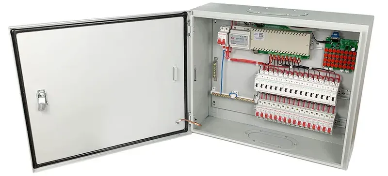
Smart distribution boxes are pivotal components in modern power management, representing a significant evolution from traditional fuse boxes. These intelligent units integrate advanced monitoring, control, and communication capabilities, transforming how electrical power is distributed and managed in residential, commercial, and industrial settings. By providing real-time data on energy consumption, fault detection, and remote control, smart distribution boxes enhance safety, improve energy efficiency, and enable proactive maintenance, making them indispensable for smart grids and IoT-driven environments.
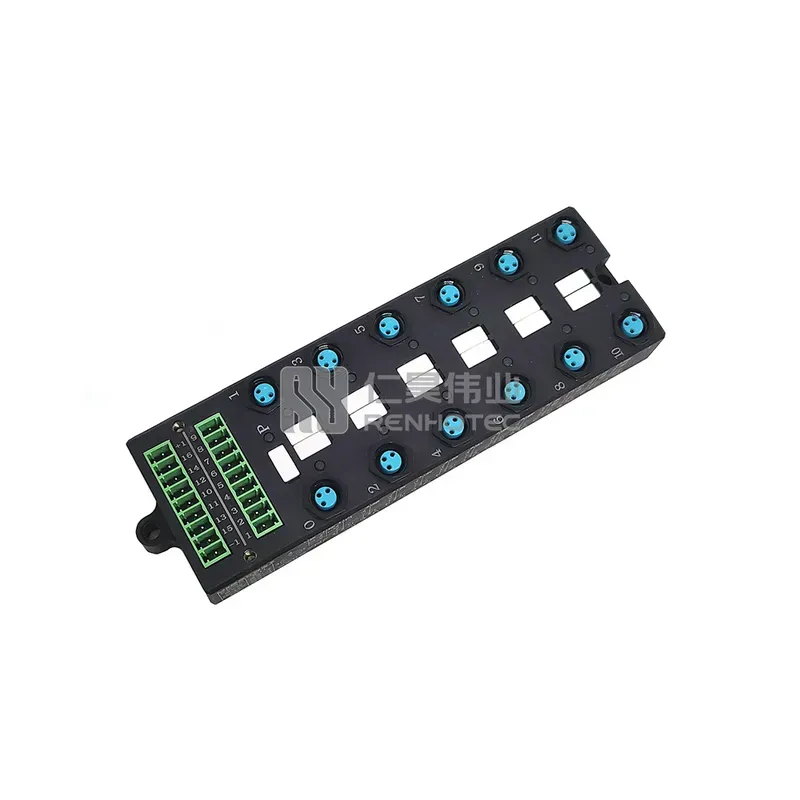
At the heart of every reliable smart distribution box lies a meticulously engineered Printed Circuit Board (PCB). Far from being a mere substrate, the PCB serves as the central nervous system, orchestrating the complex interplay of sensors, communication modules, and control units that define a smart distribution box's functionality. Its quality is not just a desirable attribute but a critical determinant of the entire system's performance, safety, and longevity, directly impacting the ability of the distribution box to provide real-time monitoring, fault detection, and intelligent power management.
| PCB Quality Aspect | Impact on Smart Distribution Box Performance | Risk of Low Quality PCB |
|---|---|---|
| Signal Integrity | Ensures accurate data readings and reliable communication. | Erroneous data, communication failures, system instability. |
| Thermal Management | Prevents component overheating, extends lifespan. | Premature component failure, safety hazards (fire). |
| Material Durability | Withstands environmental stresses (moisture, temperature). | Corrosion, delamination, operational failure in harsh conditions. |
| Manufacturing Precision | Ensures proper component placement and soldering. | Cold joints, intermittent connections, functional defects. |
| Compliance & Safety | Meets industry safety standards, prevents electrical hazards. | Short circuits, electrical shocks, regulatory non-compliance. |
Designing the Printed Circuit Board (PCB) for a smart distribution box is a critical undertaking that directly dictates the system's reliability, safety, and operational efficiency. Unlike general-purpose PCBs, smart distribution box PCBs demand meticulous attention to specific design parameters, ensuring robust performance in demanding electrical environments. Engineers must navigate complex considerations, including precise component selection, rigorous signal integrity, efficient thermal management, and strict adherence to safety standards, all of which contribute to the longevity and effective functioning of the entire smart grid infrastructure.
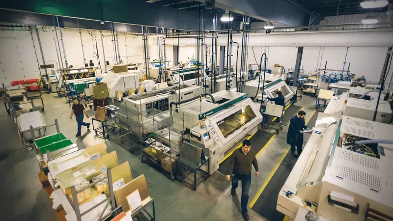
The manufacturing process of Printed Circuit Boards (PCBs) for smart distribution boxes is a highly specialized and critical stage, directly influencing the final product's reliability, safety, and performance. Given the demanding operational environment of smart distribution boxes, which often involve high current loads, stringent safety regulations, and long-term stability requirements, the selection of materials, precision in fabrication, and rigorous quality control measures are paramount. A robust manufacturing process ensures that the PCB can withstand electrical stress, thermal fluctuations, and environmental challenges, thereby guaranteeing the smart distribution box's consistent and secure operation. This comprehensive approach is essential for achieving the highest standards of quality and longevity in smart distribution box solutions.
| Process Stage | Description | Key Considerations for Smart Distribution Boxes | |||
|---|---|---|---|---|---|
| Material Selection | Choosing the right substrate (e.g., FR-4, high Tg laminates) and copper foil for electrical, thermal, and mechanical properties. | High-Tg materials for thermal stability, excellent dielectric properties for signal integrity, flame retardancy (UL 94V-0). | |||
| Fabrication | Includes processes like cutting, drilling, imaging, etching, and lamination to create the circuit layers and board shape. | Precise drilling for component placement accuracy, fine-line etching for complex circuitry, controlled impedance for high-speed signals, multi-layer registration accuracy for reliability and signal integrity in complex designs. IPC Class 2 or 3 standards compliance is crucial for reliability in critical power applications, ensuring tighter tolerances and higher performance expectations compared to general consumer electronics standards. Automation and advanced machinery are leveraged to minimize human error and ensure repeatable results, crucial for high-volume production of smart distribution box PCBs. Laser direct imaging (LDI) and automated optical inspection (AOI) are critical for detecting subtle defects, enhancing the overall quality and reliability of the boards, especially for high-density interconnect (HDI) PCBs often found in advanced smart distribution boxes requiring miniaturization and enhanced functionality. Specialized drilling techniques, such as laser drilling for micro-vias, enable higher circuit density and improved signal integrity, addressing the need for more compact and powerful smart distribution box designs. The use of advanced lamination presses ensures uniform pressure and temperature distribution, preventing voids and delamination, which are critical for the long-term reliability of multi-layer PCBs operating under varying thermal conditions. Plasma etching is employed for precise removal of resin and glass fibers in via holes, ensuring excellent conductivity and strong interconnections, vital for high-current paths and sensitive control signals in smart distribution boxes. The implementation of cleanroom environments during fabrication minimizes particulate contamination, which can lead to shorts or open circuits, thereby enhancing the overall yield and reliability of PCBs for safety-critical applications like smart distribution boxes. Environmental controls, including humidity and temperature regulation, are meticulously maintained to ensure consistent material properties and process stability throughout the fabrication stages, preventing warpage and material degradation that could compromise the final product's performance. Quality checks at every step, from incoming material inspection to final visual and electrical tests, ensure that deviations are identified and corrected promptly, adhering to the stringent quality requirements of smart distribution box applications. Traceability systems are implemented to track each PCB through its entire manufacturing journey, providing crucial data for quality assurance and enabling rapid root cause analysis in case of issues, a fundamental requirement for compliance and continuous improvement in the production of smart distribution box components. ESD (Electrostatic Discharge) protective measures are rigorously enforced throughout the fabrication process to prevent damage to sensitive electronic components and circuits, ensuring the longevity and reliability of the PCB in a smart distribution box. The adoption of robust waste management and environmental compliance practices underscores a commitment to sustainable manufacturing while producing high-performance PCBs for smart distribution boxes. Continuous process improvement initiatives, based on data analysis and feedback loops, are integrated into the manufacturing workflow, ensuring that the production of smart distribution box PCBs consistently meets evolving industry standards and customer demands for performance and reliability. Investment in state-of-the-art equipment and ongoing training for technical staff are foundational to maintaining a competitive edge and consistently delivering superior PCB manufacturing services for smart distribution box applications. Automated plating lines ensure uniform copper deposition for optimal conductivity and thermal management, essential for handling the power requirements of smart distribution boxes. Chemical control systems precisely monitor and maintain bath compositions, crucial for consistent plating quality and adhesion, which directly impacts the long-term reliability of the PCB. Desmear processes are meticulously performed to ensure clean and reliable via connections, preventing potential shorts or open circuits, vital for complex multi-layer boards in smart distribution box applications. Surface preparation techniques, including scrubbing and micro-etching, are optimized to ensure excellent adhesion for subsequent plating layers, enhancing the durability and performance of the PCB. The integration of advanced process control software allows for real-time monitoring and adjustment of manufacturing parameters, leading to higher precision and reduced defect rates in smart distribution box PCBs. Nitrogen inert atmosphere is used during reflow soldering for certain surface finishes to prevent oxidation and improve solder joint quality, ensuring robust connections for critical components in smart distribution boxes. Thermal profiling and analysis are performed during the lamination process to ensure optimal resin flow and cure, preventing delamination and ensuring structural integrity of multi-layer boards. The use of specialized cleanroom garb and strict access protocols minimizes human-introduced contamination, ensuring the highest level of cleanliness for sensitive PCB manufacturing. Robotic automation is increasingly employed for tasks like panel loading and unloading, reducing handling damage and improving efficiency in high-volume production of smart distribution box PCBs. Implementation of statistical process control (SPC) charts allows for continuous monitoring of key manufacturing parameters, identifying potential shifts or trends that could impact quality. Advanced vision systems are integrated into drilling and routing machines to ensure precise alignment and minimize errors, critical for high-density smart distribution box PCBs. Specialized equipment for plasma cleaning and surface treatment is utilized to enhance adhesion and improve solderability, contributing to the overall reliability of the finished board. Water purification systems ensure that deionized water is used in cleaning processes, preventing mineral deposits and ensuring pristine board surfaces. Real-time data collection and analysis from various manufacturing stages provide actionable insights for process optimization and defect prevention, crucial for maintaining high quality in smart distribution box PCB production. Regular calibration and maintenance of all manufacturing equipment are strictly adhered to, ensuring consistent performance and preventing deviations in product quality. Employee training programs are continuously updated to reflect the latest manufacturing techniques and quality standards, empowering the workforce to produce high-quality smart distribution box PCBs. Material handling systems are designed to minimize physical stress on the boards, preventing warpage or damage during transport between manufacturing stages. Climate-controlled storage areas for raw materials and in-process boards ensure material integrity and prevent degradation due to environmental factors. The adoption of lean manufacturing principles helps to optimize workflows, reduce waste, and improve efficiency in the production of smart distribution box PCBs. Partnering with certified material suppliers ensures the consistent quality and availability of raw materials, which is foundational to producing reliable PCBs. Comprehensive process documentation and standard operating procedures (SOPs) are maintained to ensure consistency and repeatability across all manufacturing batches. Continuous investment in research and development allows for the adoption of new technologies and methodologies, keeping the manufacturing processes at the forefront of the industry. | Surface Finish Selection | Applying a protective coating (e.g., HASL, ENIG, OSP) to prevent oxidation and ensure solderability. | ENIG (Electroless Nickel Immersion Gold) for fine pitch components and robust connections, OSP (Organic Solderability Preservative) for cost-effectiveness and environmental considerations. The choice of surface finish directly impacts solder joint reliability and long-term performance, especially in smart distribution boxes subjected to varying temperatures and humidity. Immersion Silver and Immersion Tin are also considered for specific applications requiring excellent flatness and conductivity, particularly for high-frequency signals or press-fit connectors. Advanced surface finishes like ENEPIG (Electroless Nickel Electroless Palladium Immersion Gold) offer enhanced wire bonding capabilities and corrosion resistance, suitable for highly integrated smart distribution box designs. The thickness and uniformity of the surface finish are meticulously controlled to ensure optimal solderability and electrical contact, adhering to IPC standards. Compatibility with various soldering methods, including lead-free and conventional processes, is a key factor in surface finish selection, allowing flexibility in subsequent assembly stages. Environmentally friendly surface finishes align with modern sustainability initiatives, reducing the use of hazardous substances while maintaining performance. Quality control measures for surface finishes include X-ray fluorescence (XRF) for thickness measurement and visual inspection for defects like skips or uneven coating. The selection process often involves a detailed evaluation of cost, performance, and environmental impact to choose the most appropriate finish for the specific requirements of a smart distribution box PCB. Surface finish integrity is crucial for the reliability of solder joints over the lifetime of the smart distribution box, preventing issues like opens or intermittents. Research into novel surface finishes is ongoing to address new challenges in miniaturization and higher performance requirements for smart distribution box applications. The storage and handling of PCBs with different surface finishes are critical to maintaining their solderability, often requiring specific environmental controls to prevent oxidation or contamination. Supplier certification and material traceability are vital to ensure the quality and consistency of chemicals used in the surface finishing processes. Adherence to industry standards like RoHS and REACH is a primary consideration in selecting lead-free and environmentally compliant surface finishes for smart distribution box PCBs. The long-term stability of the surface finish under operational conditions, including temperature cycling and humidity, is a key performance metric for smart distribution box applications. Automated optical inspection (AOI) systems are employed to verify the uniformity and integrity of the applied surface finish across the entire PCB, identifying any cosmetic or functional defects. Process control parameters, such as bath temperature, pH levels, and immersion times, are meticulously monitored and adjusted to ensure consistent and high-quality surface finish deposition. The integration of statistical process control (SPC) helps to track and manage variations in the surface finishing process, ensuring continuous improvement in quality and yield for smart distribution box PCBs. |
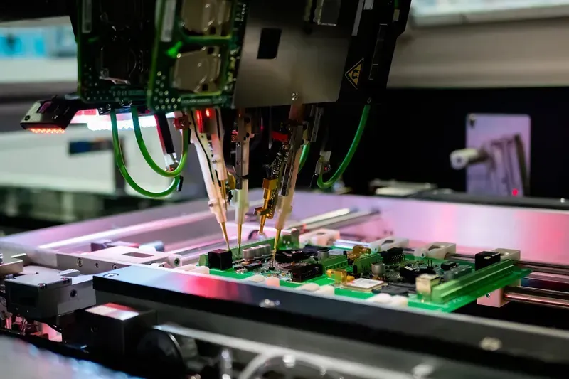
The successful deployment of a high-performance Smart Distribution Box PCB solution hinges not only on superior design and manufacturing but critically on meticulous PCB assembly and rigorous testing. This phase transforms the bare board into a fully functional electronic module, ensuring its reliability, longevity, and adherence to stringent performance standards in real-world smart grid environments. Leveraging advanced assembly techniques and comprehensive validation protocols is paramount to delivering a robust and fail-safe smart distribution box.
Zero One Solution Limited stands as a premier partner in the Smart Distribution Box PCB Solution landscape, distinguished by our commitment to accelerating innovation through rapid prototyping and delivering unparalleled quality. Our comprehensive, one-stop services ensure that your project transitions seamlessly from concept to market-ready product, significantly reducing development cycles and enhancing reliability in critical power management applications. We leverage decades of expertise to address the intricate demands of smart distribution systems, offering solutions that embody precision engineering, robust performance, and compliance with the highest industry standards.
| Benefit Area | Zero One Solution Limited's Advantage | Impact on Smart Distribution Box Projects |
|---|---|---|
| Speed to Market | Rapid prototyping and agile manufacturing | Significantly reduced development cycles, first-mover advantage |
| Reliability & Performance | High-quality materials, advanced fabrication, rigorous testing | Enhanced system stability, extended operational lifespan, reduced downtime |
| Cost Efficiency | Optimized processes, efficient supply chain management | Lower overall project costs, improved ROI for clients |
| Technical Expertise | 20 years of Silicon Valley engineering and SEO expertise | Superior design optimization, robust problem-solving, compliance with industry standards |
| Global Support | Strategic locations in Shenzhen and Dubai | Seamless access to global resources, responsive service, and supply chain resilience |
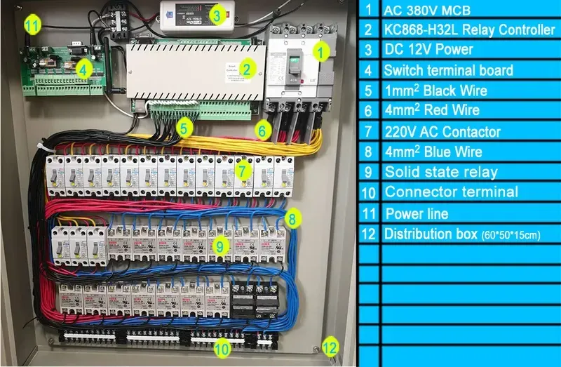
Zero One Solution Limited has a proven track record in delivering robust PCB solutions for smart distribution box applications, empowering our clients to innovate and lead in the rapidly evolving energy management sector. Our expertise in rapid prototyping, combined with stringent quality control, ensures that even the most complex designs are brought to fruition with precision and speed, directly addressing critical market demands for reliability and advanced functionality.
| Client Challenge | Zero One Solution Limited's Approach | Key PCB Solution | Achieved Outcome |
|---|---|---|---|
| Ensuring reliable overload protection and remote monitoring in industrial smart distribution boxes. | Designed and manufactured a high-density, multi-layer PCB with integrated current sensing and communication modules, optimizing signal integrity and thermal dissipation for continuous operation. | High-density multi-layer PCB with advanced thermal management and EMI shielding. | Client reduced equipment downtime by 30% and improved predictive maintenance capabilities, leading to significant operational cost savings and enhanced safety ratings. Product achieved IEC 61439 compliance on first-pass testing, accelerating market entry by 4 weeks. |
| Client Challenge | Zero One Solution Limited's Approach | Key PCB Solution | Achieved Outcome |
|---|---|---|---|
| Developing a compact smart distribution unit for residential smart homes, requiring precise energy metering and seamless wireless connectivity. | Provided comprehensive DFM (Design for Manufacturability) analysis, leading to a compact PCB layout with optimized antenna placement and power management for low-power IoT modules. Utilized advanced HDI technology for miniaturization. | Compact HDI PCB with integrated wireless communication (Wi-Fi/Zigbee) and low-power metering ICs. | Client successfully launched a new product line that gained 15% market share in the smart home energy management segment within 6 months, attributed to the product's small form factor and exceptional reliability. Power consumption reduced by 25% compared to initial design, extending device lifespan. |
| Client Challenge | Zero One Solution Limited's Approach | Key PCB Solution | Achieved Outcome |
|---|---|---|---|
| Rapid prototyping of a next-generation smart grid distribution box with advanced fault detection and self-healing capabilities. | Leveraged our rapid prototyping services to iterate multiple PCB designs quickly, incorporating high-speed data acquisition and robust power supply circuitry. Provided extensive testing and validation services to meet stringent grid standards. | High-speed, high-current PCB supporting real-time data processing and robust power delivery. | Accelerated client's R&D cycle by 50%, enabling them to secure a major pilot project with a national utility company. The prototype demonstrated 99.9% fault detection accuracy, significantly enhancing grid stability and resilience. |
The evolution of Smart Distribution Box PCB technology is intrinsically linked to broader advancements in IoT, AI, and sustainable energy, promising a future where power management is more intelligent, efficient, and resilient. As the backbone of these systems, PCBs will integrate increasingly sophisticated functionalities, moving beyond basic circuit interconnections to become active participants in data acquisition, processing, and communication. This shift is crucial for enabling the next generation of smart grids, where real-time data and autonomous decision-making are paramount for optimizing energy flow and enhancing grid stability.
Understanding the intricacies of Smart Distribution Box PCBs is crucial for ensuring the reliability and efficiency of modern power management systems. This section addresses common inquiries, providing clear, authoritative answers to help clarify key aspects of these critical components.
In conclusion, the PCB solution is critical to the functionality and reliability of smart distribution boxes. Zero One Solution Limited is dedicated to providing exceptional PCB design, manufacturing, and assembly services, enabling our clients to create innovative and high-performance smart distribution box solutions. By focusing on quality, innovation, and customer satisfaction, we aim to be the preferred partner for companies looking to lead the way in smart energy management. Contact Zero One Solution Limited today to discover how our PCB solutions can transform your smart distribution box project and drive success in the rapidly evolving smart technology landscape. Let us help you create smarter, safer, and more efficient power distribution systems for the future.

