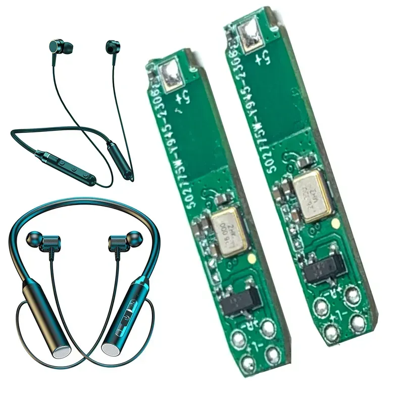
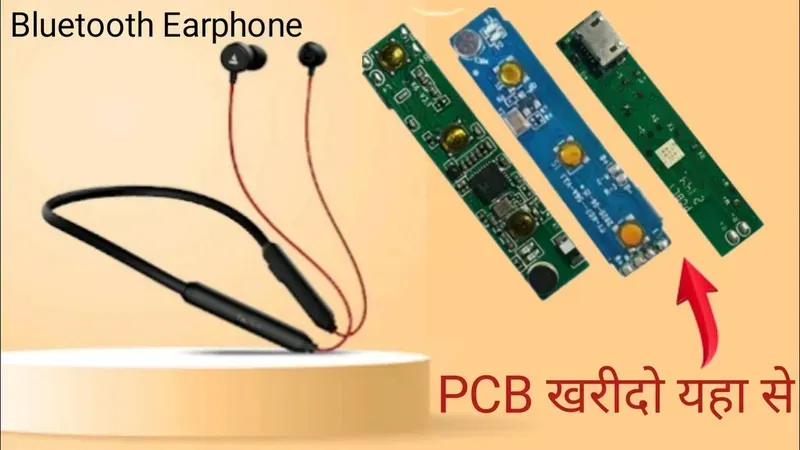
In today's fast-paced audio technology landscape, smart earphones have become more than just listening devices; they are sophisticated wearables packed with complex electronics. At the heart of every high-performing smart earphone lies its Printed Circuit Board (PCB), the silent enabler of all its functions. How do leading audio companies ensure their earphones deliver crystal-clear sound, seamless Bluetooth connectivity, and reliable performance? The answer lies in a robust and meticulously designed PCB solution. This article delves into the world of smart earphone PCB solutions, exploring the critical aspects of design, manufacturing, and assembly, and highlighting how Zero One Solution Limited is leading the charge in this innovative field.
The Critical Role of PCBs in Smart Earphones
Smart Earphone PCB
The Printed Circuit Board (PCB) serves as the fundamental backbone of smart earphones, analogous to the central nervous system, orchestrating every intricate function from immersive audio delivery to seamless wireless communication. Far from being a mere component, the PCB in smart earphones is a highly complex, miniaturized marvel of engineering, critical for integrating advanced features like active noise cancellation (ANC), voice assistants, biometric sensors, and touch controls within an incredibly confined space. Its precision directly impacts sound quality, power efficiency, and overall user experience, making its design and manufacturing paramount for competitive smart earphone products.
Signal Processing Hub The PCB acts as the central hub for all digital and analog signal processing. It precisely routes audio signals from the source to the drivers, manages digital-to-analog conversion, and handles complex algorithms for features like active noise cancellation (ANC) and spatial audio. Any compromise in PCB design can introduce noise, distortion, or latency, directly degrading the audio experience. Advanced multilayer PCBs with controlled impedance traces are essential to maintain signal integrity in such high-frequency, low-power environments.
Integrated Power Management Efficient power management is crucial for the extended battery life expected from smart earphones. The PCB meticulously manages power distribution to various components—Bluetooth modules, audio codecs, DSPs, and sensors—while ensuring minimal power loss. This involves integrating miniature power management ICs (PMICs), voltage regulators, and charging circuits. A well-designed PCB optimizes current paths and thermal dissipation, preventing hot spots and extending both battery life and component longevity, a key differentiator in a crowded market.
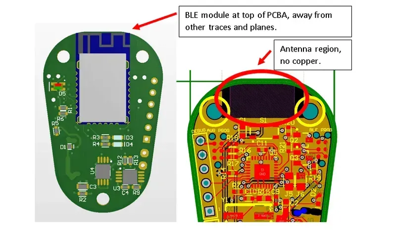
Seamless Wireless Connectivity For smart earphones, reliable wireless connectivity, primarily Bluetooth, is non-negotiable. The PCB houses the Bluetooth module and its associated antenna, demanding meticulous impedance matching and careful component placement to ensure robust signal transmission and reception. Interference from other onboard components must be mitigated through precise grounding and shielding techniques, guaranteeing stable connections and high-fidelity audio streaming, even in challenging RF environments. Future iterations may integrate UWB or Wi-Fi for enhanced capabilities.
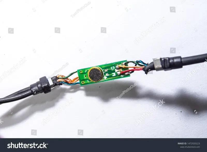
Sensor Integration & Control Modern smart earphones incorporate various sensors for advanced functionalities: accelerometers and gyroscopes for gesture control and activity tracking, proximity sensors for in-ear detection, and even bio-sensors for heart rate monitoring. The PCB provides the intricate interconnections and processing capabilities for these sensors, enabling features like automatic pausing, tap controls, and health monitoring. Miniaturization and low-power consumption are critical challenges in integrating these diverse sensor arrays without compromising form factor or battery life.
Compact & Durable Mechanical Platform Given the extremely small form factor of smart earphones, the PCB serves as the mechanical foundation upon which all other components are mounted. It must be highly compact, often utilizing High-Density Interconnect (HDI) and Any-Layer Interstitial Via Hole (ALIVH) technologies to pack maximum functionality into minimal space. Simultaneously, it must withstand daily wear and tear, including sweat, moisture, and accidental drops. Material selection (e.g., flexible PCBs, advanced FR-4 variants) and robust solder joint integrity are paramount for long-term reliability and durability in a consumer-grade product.
Key Considerations for Smart Earphone PCB Design
Earphone PCB Component Placement
Designing a printed circuit board (PCB) for smart earphones presents unique challenges, primarily driven by the demand for miniaturization, high performance, and robust functionality within an extremely confined space. The success of a smart earphone hinges significantly on an optimized PCB design that carefully balances size, component integration, thermal dissipation, and signal integrity to deliver an exceptional user experience and extended battery life. Understanding these critical considerations is paramount for engineers aiming to develop next-generation audio devices.
Design Consideration
Impact on Performance
Key Challenges and Solutions
Miniaturization & Form Factor
Enables compact, lightweight, and comfortable earphone designs.
Challenge: Limited real estate for components and traces. Solution: High-Density Interconnect (HDI) and Any-Layer HDI technology, micro-vias, and fine-line routing.
>Component Placement & Layout
Influences signal integrity, thermal management, and manufacturability.
Challenge: Crosstalk, EMI, and heat hotspots. Solution: Strategic component grouping (e.g., analog/digital separation), impedance control, and power plane optimization.
>Thermal Management
Ensures reliable operation, prevents overheating, and extends component lifespan.
Challenge: Heat dissipation in sealed, small enclosures. Solution: Copper pours for heat spreading, thermal vias, and careful consideration of component power dissipation.
>Signal Integrity (Audio & RF)
Crucial for clear audio transmission and reliable wireless connectivity.
Challenge: Noise, impedance mismatch, and attenuation. Solution: Controlled impedance traces, proper grounding, shielding, and careful routing of sensitive signals.
>Power Efficiency & Battery Life
Maximizes user playtime and minimizes charging frequency.
Challenge: High power consumption of advanced features (ANC, AI). Solution: Efficient power management ICs (PMICs), low-power components, and optimized power delivery networks (PDN).
Material Selection for Optimal Performance
Earphone PCB Material Close-Up
Selecting the right materials for Smart Earphone PCB Solutions is paramount, directly influencing signal integrity, mechanical flexibility, and long-term durability in such compact, high-performance devices. As smart earphones demand ever-smaller form factors and enhanced functionality, the choice of substrate, copper foil, and solder mask directly impacts everything from audio fidelity to battery life and product lifespan. An informed material selection ensures the PCB can withstand repetitive flexing, extreme temperatures, and provide consistent electrical performance, which is critical for consumer satisfaction and product reliability in the competitive audio market.
FR-4 is cost-effective but less flexible. Polyimide offers excellent flexibility and high-temperature resistance, crucial for rigid-flex designs. LCP provides superior high-frequency performance and low moisture absorption, ideal for advanced wireless features and harsh environments. Higher dielectric constant materials can lead to signal loss, while lower Dk/Df are preferred for high-frequency RF applications to maintain signal integrity.
Why is material selection so critical for signal integrity in smart earphone PCBs? Signal integrity, especially for high-frequency audio and wireless signals, is heavily dependent on the dielectric properties (dielectric constant, Dk; dissipation factor, Df) of the PCB substrate material. Lower Dk and Df values minimize signal loss and distortion, ensuring accurate transmission of audio data and reliable wireless connectivity. For example, a high Df can lead to more energy dissipation as heat, degrading signal quality, particularly at the gigahertz frequencies used by Bluetooth and other wireless protocols.
Advanced Manufacturing Techniques for Miniaturization
Micro PCB Manufacturing
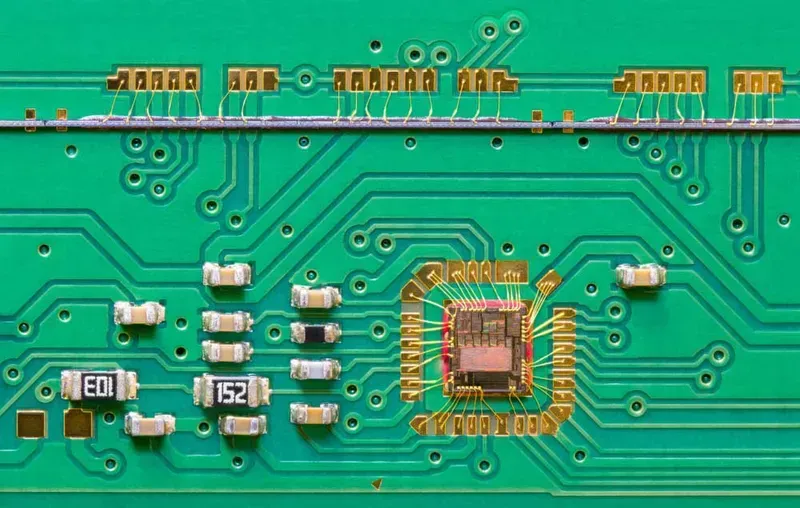
Achieving the ultra-compact form factor and high functionality demanded by modern smart earphones necessitates sophisticated PCB manufacturing techniques. Miniaturization goes beyond simply reducing size; it requires integrating more components into a smaller footprint while maintaining signal integrity and power efficiency. This is primarily accomplished through advanced approaches like High-Density Interconnect (HDI) and microvia technology, which are pivotal in creating compact, high-performance PCBs essential for cutting-edge audio devices.
High-Density Interconnect (HDI) Technology HDI PCBs represent a significant leap in circuit board design, allowing for denser component placement and improved electrical performance. By utilizing finer lines, smaller vias, and increased layer counts within a given area, HDI technology dramatically reduces the overall PCB size. This is crucial for smart earphones where space is at a premium, enabling the integration of complex features like advanced audio codecs, wireless communication modules, and power management ICs without compromising the ergonomic design.
Microvia Technology Microvias are tiny holes drilled with lasers, typically less than 150 micrometers in diameter, connecting layers within an HDI PCB. Unlike traditional through-hole vias, microvias allow for extremely fine pitch components and stacked or staggered configurations, further increasing routing density. This precision drilling minimizes board space consumption and reduces parasitic capacitance and inductance, which is vital for maintaining high-fidelity audio signals and ensuring efficient power delivery in compact earphone designs.
Build-Up Layer (BUL) Processes BUL technology, often synonymous with HDI, involves adding layers sequentially onto a core substrate. This process allows for precise control over layer thickness and material properties, facilitating the creation of complex, multi-layer PCBs with excellent signal integrity. For smart earphones, BUL enables the intricate routing required for various sensors, microphones, and wireless antennas, all within a constrained space, leading to highly integrated and feature-rich devices.
Stacked & Staggered Microvias These advanced microvia configurations maximize interconnect density. Stacked microvias are aligned directly above each other through multiple layers, while staggered microvias are offset. Both techniques reduce the need for larger, conventional vias and free up valuable surface area for component placement, contributing significantly to the miniaturization and advanced functionality of smart earphone PCBs. This allows for more compact designs without sacrificing performance or feature sets.
The adoption of these advanced manufacturing techniques by PCB solution providers like Zero One Solution Limited is fundamental to meeting the evolving demands of the smart earphone market. These innovations not only enable unprecedented miniaturization but also enhance the overall performance, reliability, and functionality of these sophisticated audio devices.
Ensuring Signal Integrity and Reducing Noise
Earphone PCB Signal Testing
In the realm of smart earphones, maintaining impeccable signal integrity and minimizing noise are paramount to delivering a superior audio experience. The PCB serves as the central nervous system, and any compromise in signal fidelity can lead to distorted sound, dropped connections, and a diminished user experience. Achieving this requires meticulous attention to design principles that mitigate interference and preserve the purity of audio signals, ensuring that the listener hears precisely what the creators intended.
Why is signal integrity so crucial for smart earphone PCBs? Signal integrity (SI) is critical because smart earphones transmit delicate analog and high-speed digital signals for audio, data, and power. Any degradation, such as reflections, crosstalk, or electromagnetic interference (EMI), can distort the audio, reduce Bluetooth range, or cause system instability, directly impacting sound quality and overall performance. Precise signal transmission is the foundation of a high-fidelity audio device, directly influencing user satisfaction and device reliability.
What are the primary sources of noise and interference in smart earphone PCBs? Noise and interference in smart earphone PCBs typically stem from several sources: electromagnetic interference (EMI) from high-frequency digital components and wireless modules (e.g., Bluetooth), power supply noise (PSN) due to ripples or fluctuations, crosstalk between adjacent traces, and ground bounce from rapid current changes. These factors can collectively degrade audio quality and system stability if not properly managed.
How does PCB layout affect signal integrity and noise reduction? PCB layout profoundly impacts signal integrity. Proper routing, such as maintaining impedance control, minimizing trace lengths, separating analog and digital grounds, and implementing effective shielding, is crucial. Strategic component placement, especially for sensitive analog circuits and high-speed digital components, also plays a vital role in reducing crosstalk and EMI, ensuring cleaner signals and reduced noise levels.
What techniques are employed to minimize noise in smart earphone PCB designs? To minimize noise, several techniques are employed: using multi-layer PCBs for better ground planes and signal isolation, implementing decoupling capacitors close to ICs to suppress power supply noise, employing differential signaling for high-speed data lines to reject common-mode noise, incorporating EMI shielding, and carefully designing power delivery networks (PDNs) to maintain stable voltage rails. These combined approaches ensure robust noise suppression.
Bluetooth and Wireless Connectivity Integration in Smart Earphone PCB Solution
Bluetooth Earphone PCB
Seamless and reliable wireless connectivity is paramount for smart earphones, and its robust integration into the PCB design is a complex engineering feat. The PCB serves as the central nervous system for wireless communication, hosting critical components like Bluetooth modules, antennas, and RF front-end circuitry. Achieving optimal performance necessitates meticulous layout design to minimize signal loss, electromagnetic interference (EMI), and ensure stable data transmission, directly impacting the user's audio experience and device responsiveness. At Zero One Solution Limited, our expertise lies in engineering PCBs that not only accommodate these advanced wireless technologies but also optimize their performance within the stringent size and power constraints of smart earphones.
What are the primary challenges of integrating Bluetooth into a compact smart earphone PCB? The primary challenges include managing electromagnetic interference (EMI) from other components, optimizing antenna placement and design within extremely limited space for reliable signal strength, minimizing power consumption to extend battery life, and ensuring robust data transmission speeds for high-fidelity audio streams and low-latency interactions. These factors necessitate careful component selection, advanced layout techniques, and thorough RF validation.
How does antenna design impact the wireless performance of smart earphones? Antenna design is critical for wireless performance. A poorly designed or placed antenna can lead to reduced range, dropped connections, and decreased audio quality. In smart earphones, where space is severely limited, custom-designed antennas (e.g., F-type, chip, or PCB trace antennas) are often integrated directly onto the PCB, requiring precise impedance matching and careful consideration of surrounding component clearances to maximize radiation efficiency and minimize interference.
What PCB design considerations are crucial for ensuring stable wireless connectivity? Crucial PCB design considerations for stable wireless connectivity include maintaining optimal impedance control for RF traces, isolating sensitive analog and digital circuitry from RF components, implementing effective grounding strategies to reduce noise, placing decoupling capacitors close to power pins, and ensuring proper thermal management for RF modules. These measures collectively prevent signal degradation and maintain connection stability.
Power Management and Battery Efficiency in Smart Earphone PCB Solutions
Optimizing power management and battery efficiency is paramount in smart earphone PCB design, directly influencing device usability, user experience, and overall market competitiveness. The compact size of smart earphones necessitates highly efficient power circuits to extend playback time, a critical factor for consumer satisfaction. Effective PCB design strategies are essential to minimize power consumption, manage heat dissipation, and ensure stable voltage delivery to sensitive audio components and wireless modules.
Power Management Challenge
PCB Design Strategy
Benefit
Limited Battery Capacity
Implement highly efficient DC-DC converters and low-dropout regulators (LDOs). Utilize power-gating techniques for inactive components.
Maximizes operational time from small batteries, extends battery life.
Miniaturization & Heat Dissipation
Employ compact, high-efficiency power ICs. Design effective thermal pathways and utilize multi-layer PCBs for heat spreading.
Prevents overheating in constrained spaces, maintains component reliability and performance.
Integrate dynamic voltage scaling (DVS) and frequency scaling (DFS). Optimize power supply routing for different functional blocks.
Adapts power consumption to specific operational demands, enhances overall system efficiency.
Charging Circuit Integration
Design robust battery management systems (BMS) with overcharge/discharge protection and precise charging control.
Ensures safe and efficient charging, prolongs battery lifespan.
Low-Power Standby
Incorporate ultra-low quiescent current components and intelligent sleep modes.
Minimizes power draw when not in active use, reduces self-discharge.
How does PCB design impact smart earphone battery life? PCB design significantly impacts battery life through component selection, layout, and power management strategies. Efficient component placement minimizes trace lengths, reducing resistive losses. Furthermore, the integration of specialized power management integrated circuits (PMICs) and the strategic routing of power and ground planes are crucial for minimizing power consumption and optimizing energy delivery to all functional blocks, directly extending operational time per charge.
What are the key power management ICs used in smart earphone PCBs? Key power management ICs (PMICs) commonly used in smart earphone PCBs include highly efficient DC-DC converters for voltage regulation, low-dropout regulators (LDOs) for noise-sensitive analog circuits, battery charger ICs for safe and efficient charging, and fuel gauge ICs for accurate battery level reporting. These components are selected for their small form factor, high efficiency, and low quiescent current.
How do you minimize power loss due to signal interference in smart earphone PCBs? Minimizing power loss due to signal interference involves meticulous PCB layout techniques. This includes careful impedance matching, proper grounding schemes (e.g., solid ground planes), and effective shielding of sensitive analog and RF sections. Additionally, segregating power and ground lines for different functional blocks and using decoupling capacitors strategically helps reduce noise propagation, ensuring stable power delivery and preventing energy waste from signal integrity issues.
What role does material selection play in battery efficiency for smart earphone PCBs? Material selection plays a crucial role. For instance, using low-loss dielectric materials for the PCB substrate reduces signal attenuation, particularly at higher frequencies (like Bluetooth), thus conserving power. Materials with good thermal conductivity are also vital for dissipating heat generated by power components, preventing efficiency drops due to elevated temperatures and ensuring stable operation and extended component lifespan.
What advanced techniques are used to extend battery life in smart earphone PCBs? Advanced techniques include implementing dynamic voltage and frequency scaling (DVFS) to adjust power consumption based on workload, advanced power-gating for unused circuits, and integrating ultra-low power microcontrollers and DSPs. Furthermore, sophisticated firmware algorithms work in conjunction with the PCB design to optimize power states and intelligently manage component activity, maximizing operational endurance.
Zero One Solution Limited: Your Partner in Smart Earphone PCB Solutions
Zero One Solution Limited stands as a premier partner for smart earphone PCB solutions, offering a seamless, one-stop service that encompasses everything from initial design and rapid prototyping to full-scale manufacturing and precise assembly. Our deep expertise in high-density interconnect (HDI) and advanced material handling ensures that every smart earphone PCB we deliver meets the stringent demands for miniaturization, high performance, and reliability in the rapidly evolving audio wearable market.
Comprehensive Design and Layout Services Leveraging decades of experience, our engineers provide meticulous PCB design and layout services specifically tailored for smart earphones. This includes optimizing component placement for signal integrity, ensuring efficient power distribution, and designing compact layouts to fit the diminutive form factors of modern audio devices. We prioritize DFM (Design for Manufacturability) from the outset to streamline production and reduce costs. According to industry reports, a well-optimized PCB design can reduce manufacturing errors by up to 20% and accelerate time-to-market by 15% for complex electronics like smart earphones (Source: IPC Standards and Practices Survey, 2022).
Rapid Prototyping and Iteration Our rapid prototyping capabilities are a cornerstone of our service, enabling swift iteration and validation of designs. This agile approach significantly compresses development cycles, allowing clients to quickly test and refine their smart earphone concepts. With our state-of-the-art facilities in Shenzhen, a global hub for electronics manufacturing, we can turn around complex prototypes in days, not weeks. This speed is crucial for gaining a competitive edge in the fast-paced consumer electronics sector, where early market entry can significantly impact product success and market share (Source: Deloitte Technology Trends Report, 2023).
Advanced Manufacturing and Assembly Zero One Solution Limited employs cutting-edge manufacturing techniques, including HDI technology for multi-layer boards and microvia drilling, essential for the compact and feature-rich PCBs found in smart earphones. Our assembly processes are optimized for precision and efficiency, handling intricate surface-mount components (SMD) with exceptional accuracy. We adhere to rigorous quality control standards, ensuring every PCB meets the highest levels of performance and durability, critical for consumer electronics that undergo daily use. Our robust supply chain network, extending from Shenzhen to Dubai, guarantees access to top-tier materials and components, maintaining consistent quality across all production volumes.
Rapid Prototyping for Accelerated Product Development
In the fast-evolving smart earphone market, the ability to rapidly prototype Printed Circuit Boards (PCBs) is not just an advantage; it's a fundamental necessity for accelerating product development and gaining a competitive edge. Rapid prototyping allows engineers to quickly validate designs, test functionalities, and iterate on improvements, significantly reducing time-to-market and ensuring that innovative audio solutions reach consumers faster. This iterative process is crucial for refining complex features such as advanced audio processing, seamless wireless connectivity, and sophisticated power management, all while maintaining the stringent miniaturization and performance requirements of smart earphones.
How does rapid PCB prototyping benefit smart earphone development? Rapid PCB prototyping enables quick iteration and testing of design concepts, allowing for early identification and rectification of potential issues related to signal integrity, power efficiency, and component placement. This accelerated feedback loop significantly shortens the development cycle, reduces costs associated with design revisions, and ensures the final product meets stringent performance and miniaturization requirements crucial for smart earphones. It transforms months of traditional development into weeks, fostering innovation and quicker market entry.
Benefit
Traditional PCB Development
Rapid PCB Prototyping
Time-to-Market
Long, due to sequential design, testing, and revision phases
Significantly reduced, enabling concurrent engineering and faster iterations
Cost Efficiency
Higher, due to costly late-stage design changes and extensive retooling
Lower, by identifying and correcting issues early, minimizing rework and scrap
Innovation Cycle
Slower, limiting the number of design experiments and feature implementations
Accelerated, encouraging more frequent design iterations and feature experimentation
Risk Mitigation
Higher risk of unforeseen issues surfacing late in the development process
Lower risk, as design flaws and performance bottlenecks are identified and addressed proactively
At Zero One Solution Limited, our expertise in rapid-response R&D prototype manufacturing for smart earphone PCBs is a cornerstone of our service. By leveraging advanced manufacturing techniques and a deep understanding of audio electronics, we empower our clients to transform their innovative concepts into tangible prototypes with unmatched speed and precision. This capability is vital for smart earphone developers who must navigate complex design challenges while maintaining a keen eye on market trends and consumer demands. Our commitment to rapid prototyping ensures that our partners can swiftly bring cutting-edge smart earphone products to market, staying ahead in a highly competitive industry.
In conclusion, the PCB is the nerve center of any smart earphone, and its design and manufacturing are crucial to the device's overall performance and reliability. Zero One Solution Limited is committed to providing cutting-edge PCB solutions that enable our clients to create innovative and high-quality smart earphones. By focusing on rapid prototyping, advanced technology, and comprehensive services, we empower our clients to stay ahead in the competitive audio market. Contact us today to discover how our smart earphone PCB solutions can transform your product development process and bring your innovative ideas to life. Share this article and leave a comment below to let us know your thoughts on the future of smart earphone technology!