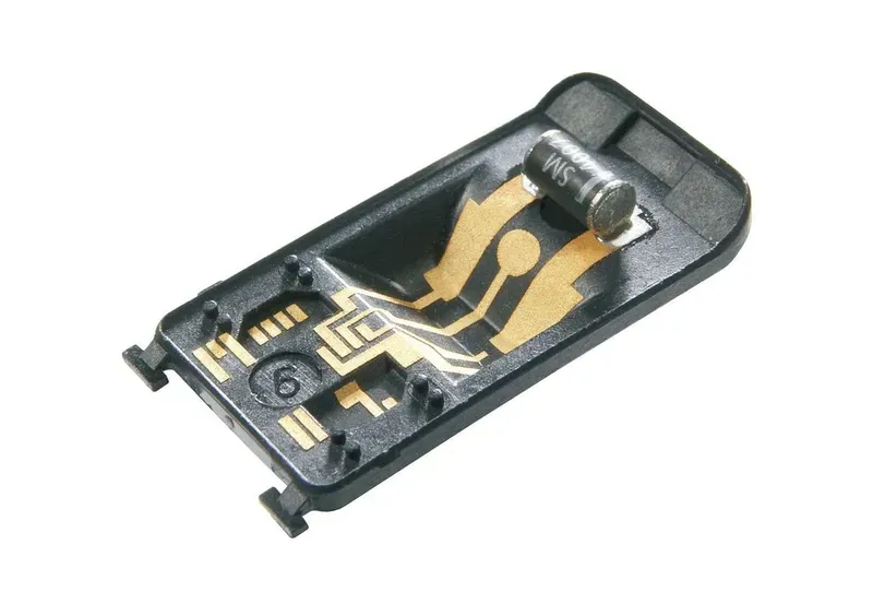
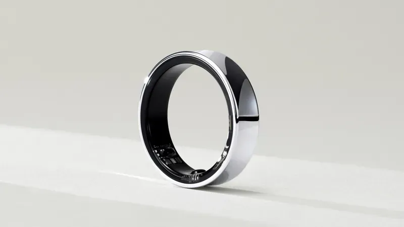
In an era where technology seamlessly integrates into our daily lives, the smart ring stands out as a marvel of miniaturization and functionality. These tiny wearable devices pack a surprising amount of technology into a compact form factor, enabling features like contactless payments, health tracking, and smartphone notifications. At the heart of every smart ring lies its Printed Circuit Board (PCB), the unsung hero responsible for connecting all the electronic components and enabling the ring's intelligent functions. Zero One Solution Limited stands at the forefront of providing specialized PCB solutions for smart rings, offering expertise in design, manufacturing, and assembly. We understand the unique challenges and requirements of creating PCBs for wearable technology, and we're committed to helping our clients bring their innovative smart ring designs to life. This article delves into the intricacies of smart ring PCB solutions, exploring the design considerations, manufacturing processes, and the critical role Zero One Solution plays in this exciting field.
Introduction to Smart Ring Technology and PCB Importance
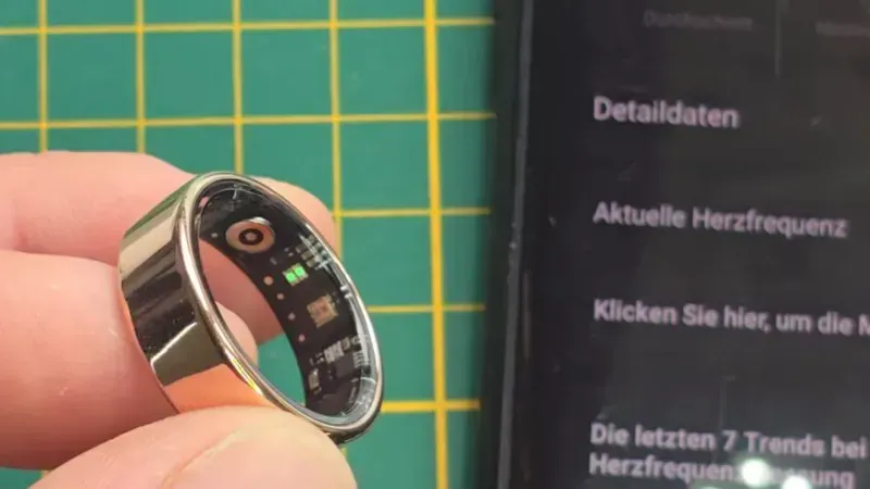
Smart Ring Internal PCB
Smart ring technology represents a significant leap in wearable innovation, integrating sophisticated electronics into a compact, stylish form factor. These miniature powerhouses offer a discreet yet powerful interface for health monitoring, contactless payments, access control, and seamless smart device interaction. At the heart of every smart ring lies its Printed Circuit Board (PCB), a marvel of miniaturization and engineering precision that dictates the device's functionality, performance, and reliability. The demand for these unobtrusive smart devices is accelerating, driven by advancements in sensor technology and battery efficiency, making the design and manufacturing of ultra-compact, high-density PCBs paramount for market success.
Understanding Smart Ring Functionality Smart rings are sophisticated wearable devices, typically worn on a finger, that integrate various sensors, communication modules (like Bluetooth Low Energy or NFC), and processing units to offer a range of functionalities. These can include continuous health monitoring (heart rate, sleep patterns, activity tracking), secure contactless payments, digital access control, and gestural control for connected devices. Their appeal lies in their subtlety, long battery life, and constant, non-intrusive data collection.
The Global Smart Ring Market Landscape The smart ring market is experiencing robust growth, fueled by increasing consumer interest in wearable technology, particularly in health and wellness. According to a report by Global Market Insights, the global smart ring market size was valued at over USD 250 million in 2022 and is projected to surpass USD 1.5 billion by 2032, exhibiting a compound annual growth rate (CAGR) of over 20%. This expansion is largely attributed to technological advancements, rising disposable incomes, and the continuous introduction of new applications that enhance user experience and convenience.
The PCB's role in a smart ring cannot be overstated. Given the extremely confined space, every millimeter counts. The PCB must not only house a diverse array of components—from minuscule sensors and power management ICs to RF antennas and memory chips—but also ensure their seamless interconnection and optimal signal integrity. This demands an unparalleled level of miniaturization, often utilizing advanced techniques such as System-in-Package (SiP) and flex-rigid PCB designs to bend and conform to the ring's curvilinear shape. Moreover, the PCB's material composition and layout are crucial for thermal dissipation and electromagnetic compatibility (EMC), ensuring the ring operates efficiently and safely against the user's skin. Reliability in a device subjected to daily wear and potential environmental stressors further underscores the critical importance of a robust and meticulously engineered PCB.
Design Challenges for Smart Ring PCBs
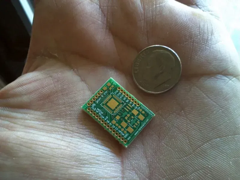
Miniature PCB Circuit
Designing PCBs for smart rings presents a unique set of engineering hurdles, primarily driven by the imperative for extreme miniaturization without compromising performance. Unlike conventional PCBs, smart ring applications demand a delicate balance of form factor, functionality, and durability within an incredibly confined space. Successfully navigating these challenges is paramount to creating a viable, high-performing wearable device, which often requires innovative material science, advanced layout techniques, and meticulous thermal considerations to ensure long-term reliability.
Size Constraints and Miniaturization The most significant challenge in smart ring PCB design is the severe space limitation. The PCB must conform to the ring's narrow, curved form factor, necessitating ultra-compact designs. This demands highly integrated components, multi-layer boards, and advanced routing strategies to pack maximum functionality into minimal volume, often pushing the boundaries of current manufacturing capabilities to achieve high-density interconnects (HDIs).
Component Density and Placement To integrate various sensors (heart rate, SpO2, NFC, accelerometers), power management ICs, Bluetooth modules, and microcontrollers within the tiny footprint, component density becomes critical. Strategic placement is essential to minimize signal interference, optimize power delivery, and ensure proper thermal dissipation, often requiring sophisticated simulation tools to validate layouts before manufacturing. Every millimeter counts, making component selection and footprint optimization a meticulous process, often favoring system-in-package (SiP) or chip-on-board (CoB) solutions for further integration and size reduction. This tight integration also increases the complexity of debugging and rework if issues arise after assembly.
Material Selection for Optimal Performance
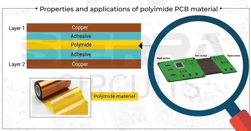
Flexible PCB Material
Selecting the right materials is paramount for the optimal performance and longevity of a Smart Ring PCB. The compact nature and continuous wear of smart rings demand substrates that excel in electrical integrity, mechanical robustness, and efficient thermal dissipation. This meticulous material selection directly influences the ring's functionality, battery life, and user comfort, making it a critical phase in the design and manufacturing process.
Material Type
Key Properties
Smart Ring PCB Application Advantages
FR-4 (Standard Epoxy Laminate)
Good electrical insulation, cost-effective, widely available
Suitable for less constrained designs or as a base for HDI layers, offering a balance of performance and cost. However, its rigidity limits advanced miniaturization and flexibility demands of smart rings.
High-Frequency Laminates (e.g., Rogers, Arlon) These materials are crucial for smart rings incorporating advanced wireless communication protocols (e.g., Bluetooth LE, NFC, Wi-Fi). Their low dielectric loss and stable dielectric constant at high frequencies ensure reliable signal transmission and minimal power consumption, which is vital for maintaining connectivity and extending battery life in a miniature device like a smart ring. Brands like Rogers 4000 series and Arlon materials are frequently chosen for their superior RF performance, enabling robust data transfer and communication within the confined space of the ring and with external devices.
Material Type
Key Properties
Smart Ring PCB Application Advantages
Flexible PCB Materials (e.g., Polyimide)
Excellent flexibility, high temperature resistance, thin profiles
Indispensable for form-fitting designs and maximizing component density in the ring's limited volume. Polyimide, in particular, allows for dynamic bending and folding, enabling complex, multi-layered circuits to conform to the ring's curvature. This flexibility is key to integrating a multitude of sensors and chips without increasing the ring's overall size, while also enhancing durability against everyday wear and tear. Its thermal stability also ensures reliable operation across varying ambient temperatures.
Advanced Substrate Materials (e.g., Liquid Crystal Polymer - LCP) LCP stands out for its exceptional dimensional stability, extremely low moisture absorption, and superior high-frequency performance, making it an ideal choice for the most demanding smart ring applications. Its ability to maintain structural integrity under varying environmental conditions and its excellent electrical properties at very high frequencies support the integration of advanced sensors and communication modules that require precise signal characteristics. Furthermore, LCP's thermal expansion coefficient is very close to that of copper, minimizing stress on solder joints during temperature cycles, thus enhancing the long-term reliability of the PCB in a device exposed to body heat and external temperature fluctuations.
Zero One Solution's Expertise in Smart Ring PCB Design
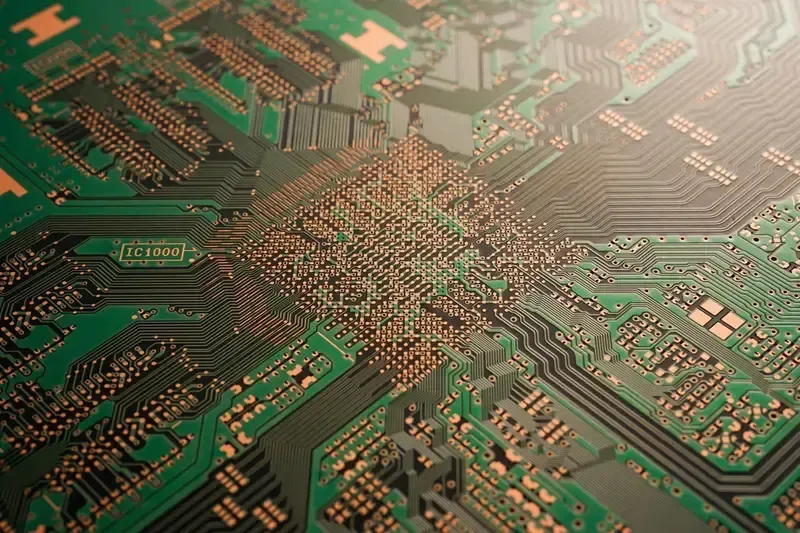
PCB Design Miniaturization
At Zero One Solution, our expertise in Smart Ring PCB design is rooted in a deep understanding of the unique challenges presented by miniaturization and high-performance demands. We leverage over a decade of experience in rapid prototyping and high-density interconnect (HDI) technologies to deliver bespoke PCB solutions that are not only compact and robust but also excel in signal integrity and power efficiency, critical for the seamless operation of smart wearables.
Miniaturization Techniques We excel in implementing advanced miniaturization techniques, including ultra-fine line and space technology (down to 25µm), stacked micro-vias, and advanced substrate materials. Our engineers utilize state-of-the-art design software for optimal component footprint reduction and efficient circuit routing, ensuring maximum functionality within the smallest possible form factor.
Component Placement Strategies Strategic component placement is paramount for Smart Ring PCBs. Our approach optimizes space utilization while mitigating electromagnetic interference (EMI) and ensuring efficient thermal dissipation. We meticulously plan the layout of sensitive components like sensors, antennas, and power management ICs to prevent signal degradation and enhance overall device performance.
Signal Integrity (SI) and Power Integrity (PI) Analysis Maintaining signal and power integrity is critical for reliable data transmission and stable operation in high-frequency smart ring applications. We conduct exhaustive SI/PI simulations using industry-leading tools to identify and mitigate potential issues such as impedance mismatches, crosstalk, and power supply noise, ensuring robust and error-free communication pathways.
Thermal Management Solutions Given the compact nature of smart rings, effective thermal management is essential to prevent overheating and ensure component longevity. Our design team incorporates innovative thermal dissipation strategies, including optimized copper pours, thermal vias, and careful material selection, to maintain optimal operating temperatures even under continuous use.
Design Capability
Zero One Solution Expertise
Benefit for Smart Ring PCB
Minimum Trace/Space
25µm (1 mil)
Enables extreme miniaturization and higher component density.
Via Technology
Stacked Micro-vias, Blind/Buried Vias
Maximizes routing space and improves signal path efficiency.
Layer Count
Up to 24 Layers
Accommodates complex circuitry for multi-functional smart rings.
Impedance Control Tolerance
±5%
Ensures high-speed signal integrity and reliable data transmission.
Thermal Management
Optimized Copper Pours, Thermal Vias, Material Selection
Prevents overheating, enhancing component lifespan and device reliability.
Advanced Manufacturing Techniques for High-Density PCBs
Laser Direct Structuring LDS
Manufacturing high-density Printed Circuit Boards (PCBs) for smart rings demands cutting-edge techniques to accommodate miniaturization and complex functionalities. These advanced processes are crucial for achieving the intricate circuitry, reliability, and performance required in such compact wearable devices. Unlike traditional PCB fabrication, smart ring PCBs necessitate precision at a microscopic level, ensuring signal integrity and robust physical integration within the confined space of a ring.
Laser Direct Structuring (LDS) LDS is a revolutionary process that allows for the direct creation of circuit traces on 3D molded plastic parts using a laser. This eliminates the need for traditional flat PCBs, enabling highly compact and uniquely shaped circuitry. For smart rings, LDS is invaluable as it integrates antennas and other electronic components directly onto the device's casing, maximizing space utilization and design flexibility. The process begins with a special polymer compound that contains a laser-activatable additive; the laser selectively activates the additive, making the treated areas metallizable for subsequent copper plating. This results in precise, durable, and highly integrated conductive paths ideal for miniaturized wearables. According to a report by Yole Développement, the global market for 3D MID (Molded Interconnect Device) including LDS is projected to grow significantly, highlighting its increasing adoption in compact electronic devices due to its space-saving and design freedom advantages.
Micro-via Drilling Micro-vias are extremely small holes (typically less than 150 microns in diameter) that connect different layers of a PCB. They are essential for high-density interconnect (HDI) PCBs found in smart rings, allowing for more complex routing and increased component density. Laser drilling is the primary method for creating these micro-vias, offering exceptional precision and the ability to drill through various dielectric materials with minimal heat damage. These tiny connections are critical for managing the high signal speeds and complex data flows within a smart ring, ensuring reliable communication between its numerous integrated sensors and processors. The IPC-2226 standard (Sectional Design Standard for High Density Interconnect (HDI) Printed Boards) emphasizes the importance of micro-vias in achieving high circuit density.
Manufacturing Technique
Application in Smart Ring PCBs
Key Advantage
Laser Direct Structuring (LDS)
Direct circuit integration on 3D plastic housing, antenna creation.
Maximized space utilization, complex 3D forms, design flexibility
Micro-via Drilling
Interconnecting layers in HDI PCBs, increasing component density.
Enables complex routing, higher component count, enhanced signal integrity
Quality Control and Reliability Testing for Smart Ring PCB Solutions
Ensuring the unwavering performance and longevity of smart ring PCBs is paramount, necessitating stringent quality control and reliability testing procedures. At Zero One Solution, our comprehensive approach goes beyond mere compliance, embedding a culture of excellence to guarantee that every smart ring PCB solution we deliver meets the highest standards of durability and functionality, thereby mitigating potential failures and enhancing user experience.
Why is rigorous quality control essential for Smart Ring PCBs? Smart ring PCBs operate within extremely confined spaces and are subjected to constant wear, environmental exposure, and high-density electrical demands. Rigorous quality control is essential to identify and rectify microscopic defects, ensure signal integrity, prevent thermal issues, and guarantee long-term performance under these challenging conditions. Without it, the compact nature of smart rings would amplify any design or manufacturing flaw, leading to premature device failure or inaccurate data.
What industry standards and certifications are relevant to Smart Ring PCB reliability? Key industry standards include IPC-A-610 (Acceptability of Electronic Assemblies) for visual inspection, IPC-TM-650 (Test Methods Manual) for various material and product tests, and ISO 9001 (Quality Management Systems) for overall quality assurance. For medical or wearable devices, specific certifications like ISO 13485 (Medical Devices Quality Management Systems) or IEC 60601 (Medical Electrical Equipment) might also be relevant, ensuring compliance with strict safety and performance benchmarks.
How does Zero One Solution ensure the reliability of Smart Ring PCBs during the manufacturing process? Zero One Solution employs a multi-faceted approach, integrating in-line quality checks at every stage, from material selection to final assembly. This includes Automated Optical Inspection (AOI) for defect detection, X-ray inspection for internal solder joint integrity, Electrical Test (E-Test) for circuit continuity and shorts, and statistical process control (SPC) to monitor and optimize manufacturing parameters. Our processes are designed to proactively identify and eliminate potential failure points.
Testing Method
Purpose for Smart Ring PCBs
Benefit
Thermal Cycling Test
Simulates temperature fluctuations encountered during daily use.
Ensures solder joint integrity and material stability under varying thermal conditions.
Vibration/Shock Testing
Evaluates structural integrity under mechanical stress.
Confirms component retention and PCB resilience against accidental drops or impacts.
Humidity Testing
Assesses performance in high-moisture environments.
Verifies moisture resistance, preventing corrosion and electrical shorts in humid conditions.
Case Studies: Successful Smart Ring Projects
Smart Ring Prototype Sample
At Zero One Solution Limited, our commitment to innovation and precision has been instrumental in the realization of cutting-edge smart ring technologies. Through rigorous design, advanced manufacturing, and meticulous quality control, we have empowered numerous clients to transform ambitious concepts into market-ready products. These case studies underscore our expertise in overcoming complex PCB challenges inherent in smart ring development, delivering compact, high-performance, and reliable solutions.
Case Study 1: Ultra-Compact Biometric Smart Ring A startup aimed to develop an ultra-thin smart ring capable of continuous biometric monitoring (heart rate, SpO2). The primary challenge was integrating multiple sensors, a microcontroller, and a power management unit within a 2mm thick PCB, requiring extreme miniaturization and precise signal routing. Zero One Solution utilized advanced HDI techniques, including 0.1mm micro-vias and fine-line etching (2/2 mil trace/space), combined with custom-designed flex-rigid PCB technology. This enabled the client to achieve an unprecedented form factor while maintaining robust performance, leading to successful product launch and significant market traction due to its comfort and functionality.
Case Study 2: NFC-Enabled Payment and Access Control Ring A client required a smart ring for secure NFC-based payments and access control, demanding robust signal integrity for NFC communication and extended battery life. The challenge involved optimizing the antenna design on a constrained PCB layout and minimizing power consumption across all integrated circuits. Our engineers implemented a multi-layer PCB stack-up with optimized ground planes and strategically placed NFC antenna coils. Through meticulous impedance matching and low-power component selection, we delivered a PCB solution that ensured reliable NFC performance and achieved over 7 days of standby battery life, surpassing the client's initial specifications and enabling rapid deployment in secure payment systems.
The Future of Smart Ring PCBs: Trends and Innovations
The trajectory of smart ring technology is intrinsically linked to advancements in Printed Circuit Board (PCB) miniaturization and integration. As consumer demand for more sophisticated functionalities within ever-smaller form factors intensifies, the future of smart ring PCBs hinges on revolutionary materials, manufacturing processes, and design paradigms. This evolution is driven by the imperative to achieve unprecedented levels of integration, flexibility, and power efficiency, unlocking new possibilities for wearable technology.
What are the key emerging trends in smart ring PCB technology? Key trends include the widespread adoption of flexible and stretchable PCBs, enhanced sensor integration at the substrate level, the development of ultra-low-power components, and the use of advanced packaging techniques like System-in-Package (SiP) and Chip-on-Flex (CoF). Furthermore, the exploration of bio-compatible materials and the integration of AI at the edge are significant advancements.
How will flexible and stretchable PCBs impact future smart rings? Flexible and stretchable PCBs are transformative for smart rings, enabling seamless conformity to the user's finger, improving comfort and durability. This allows for more intricate designs, higher component densities within constrained spaces, and better signal integrity by minimizing stress on connections during everyday use. They are crucial for integrating more sensors and power solutions without increasing the ring's bulk.
What role do advanced materials play in the evolution of smart ring PCBs? Advanced materials are fundamental to future smart ring PCBs. This includes novel dielectric substrates with improved thermal dissipation and high-frequency performance, conductive inks for printed electronics, and biocompatible polymers for direct skin contact applications. These materials facilitate thinner, lighter, and more robust PCBs capable of housing complex circuitry while meeting stringent safety and comfort standards.
Innovation Area
Current State
Future Impact
Flexible & Stretchable PCBs
Limited adoption, mostly rigid-flex
Ubiquitous, enabling seamless form factors and enhanced durability
Integrated Sensors
Discrete components, limited types
Embedded directly into PCB substrate, diverse bio-metric and environmental sensing
Power Management
Small batteries, efficiency focus
Energy harvesting (kinetic, thermal), advanced micro-batteries for extended life
Manufacturing Processes
Standard SMT, fine-line etching
Additive manufacturing, 3D printing of circuitry, direct laser patterning
Communication
Bluetooth LE
Ultra-wideband (UWB), NFC for enhanced security and data transfer
The ongoing miniaturization and functional enhancement of smart rings will continue to push the boundaries of PCB technology. Zero One Solution is at the forefront of this evolution, leveraging our rapid prototyping capabilities and deep expertise in high-density interconnect (HDI) and advanced materials to anticipate and meet the demands of future smart ring designs. Our commitment to innovation ensures that we provide cutting-edge PCB solutions that are not only compact and powerful but also reliable and scalable for mass production.
Why Choose Zero One Solution for Your Smart Ring PCB Needs?
Choosing the right partner for your smart ring PCB development is paramount to bringing innovative, reliable, and market-ready products to life. Zero One Solution Limited stands as a leading expert in providing comprehensive, end-to-end PCB solutions specifically tailored for the intricate demands of smart ring technology, from concept to mass production. Our dedication to precision engineering, cutting-edge manufacturing, and unwavering quality assurance ensures that your smart ring devices are powered by the most advanced and dependable PCB foundations.
Unrivaled Expertise in Miniaturization Zero One Solution has over a decade of specialized experience in designing and manufacturing ultra-compact, high-density PCBs essential for smart rings. Our engineers leverage advanced techniques like HDI, micro-vias, and fine-line technology to maximize functionality within the incredibly small form factor, ensuring optimal performance without compromise on size.
Commitment to Superior Quality and Reliability Quality is at the core of our operations. We adhere to stringent IPC standards and implement rigorous multi-stage quality control protocols, including AOI, X-ray inspection, and functional testing. This meticulous approach guarantees that every smart ring PCB we produce is robust, reliable, and performs consistently under diverse conditions, minimizing field failures and enhancing user satisfaction.
Accelerated Rapid Prototyping Services Understanding the fast-paced nature of smart device development, Zero One Solution excels in rapid prototyping. Our streamlined processes and advanced manufacturing capabilities enable quick turnaround times for your smart ring PCB prototypes, allowing for faster iterations, quicker validation, and significantly reducing your time-to-market.
Competitive Pricing without Compromising Excellence Strategically located in Shenzhen, China's electronic manufacturing hub, and with a global supply chain network, we offer highly competitive pricing for our smart ring PCB solutions. This cost efficiency does not come at the expense of quality or service; instead, it provides our clients with a significant competitive advantage in the smart wearables market.
In conclusion, the smart ring represents a remarkable convergence of technology and personal style. The PCB within is a critical component, demanding precision, miniaturization, and reliability. Zero One Solution Limited is dedicated to providing cutting-edge PCB solutions that empower our clients to create innovative and functional smart rings. From initial design to final assembly, we offer the expertise and resources needed to navigate the complexities of wearable technology. Contact us today to learn more about how we can help you bring your smart ring vision to reality and stay ahead in the competitive wearable tech market. Share this article with your network and leave your comments below!