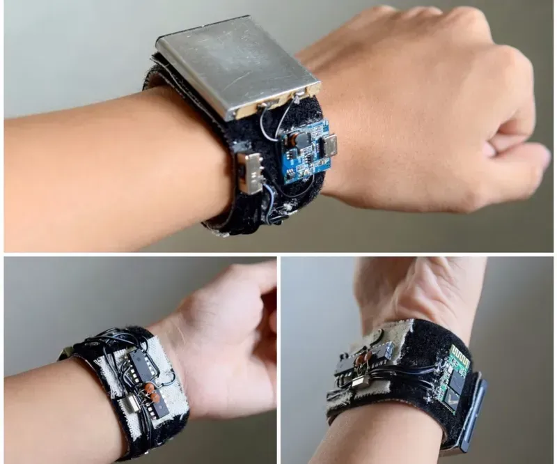
In today's fast-paced world, wearable technology has revolutionized how we monitor our health and fitness. At the heart of these devices lies the Printed Circuit Board (PCB), the unsung hero ensuring seamless functionality. This article delves into the critical role of PCB solutions in wearable heart rate monitor bands, exploring design considerations, manufacturing processes, and the expertise Zero One Solution Limited brings to this cutting-edge field. Just as the intricate network of veins and arteries supports the human body, the PCB acts as the central nervous system for these life-monitoring wearables.
Introduction to Wearable Heart Rate Monitor Bands
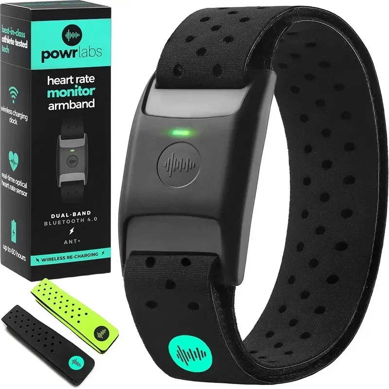
Wearable Heart Rate Monitor Band
Wearable heart rate monitor bands have emerged as indispensable tools, bridging the gap between personal health management and cutting-edge technology. These compact, sophisticated devices, powered by intricately designed Printed Circuit Boards (PCBs), are revolutionizing how individuals monitor their cardiovascular health, optimize fitness regimes, and proactively manage well-being. Their pervasive adoption underscores a fundamental shift towards personalized, real-time health data, making them central to contemporary health and fitness ecosystems.
Applications in Health and Fitness Beyond simple pulse tracking, wearable heart rate monitors offer a spectrum of applications. Athletes utilize them for performance optimization, tracking training zones, recovery rates, and identifying overtraining risks. For general wellness, they provide crucial insights into daily activity levels, sleep quality, and stress responses, enabling users to make informed lifestyle adjustments. In healthcare, these devices are increasingly leveraged for remote patient monitoring, early detection of cardiac anomalies, and post-operative recovery tracking, offering continuous, non-invasive data collection that enhances diagnostic accuracy and patient care, particularly for conditions like atrial fibrillation (AFib).
Core Benefits for Users The primary benefits of wearable heart rate monitors lie in their accessibility and precision. They empower users with actionable data, fostering a proactive approach to health. Real-time feedback on heart rate, calorie burn, and activity intensity allows for immediate adjustments during exercise. Long-term data trends provide valuable insights into cardiovascular health improvements or potential concerns, facilitating more effective communication with healthcare providers. Furthermore, the discreet and comfortable design ensures continuous wear, capturing a comprehensive physiological picture that traditional, episodic health check-ups often miss. According to a 2023 report by Statista, the global wearable technology market, largely driven by health and fitness trackers, is projected to reach over 150 billion U.S. dollars by 2026, highlighting the escalating demand and integration of these devices into daily life.
The Crucial Role of PCBs in Wearable Devices
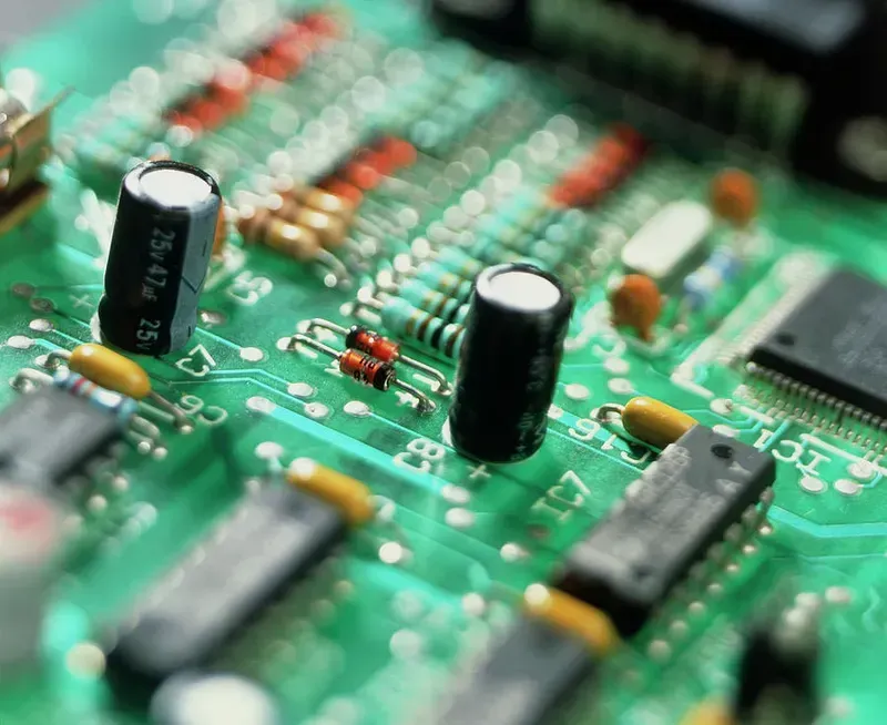
PCB Circuit Board
Printed Circuit Boards (PCBs) are the indispensable backbone of all modern electronic devices, and their role becomes even more critical within the constrained and dynamic environment of wearable technology. For devices like wearable heart rate monitor bands, PCBs serve as the miniaturized, high-density platform that integrates all electronic components, ensuring seamless functionality, efficient power distribution, and reliable data transmission. Without a meticulously designed and manufactured PCB, the compact, intelligent, and performance-driven nature of wearable devices would be unattainable, making them the silent architects of connectivity and health monitoring.
Component Integration and Miniaturization PCBs facilitate the densely packed arrangement of microcontrollers, sensors, communication modules, and power management units within the minimal footprint of a wearable device. Advanced PCB fabrication techniques, such as High-Density Interconnect (HDI) and System-in-Package (SiP), are crucial for achieving the necessary miniaturization without compromising performance, allowing for sleeker designs and enhanced user comfort.
Signal Integrity and Noise Reduction In medical and fitness monitoring, precise signal integrity is paramount. PCBs provide a stable and controlled electrical environment that minimizes signal loss, interference, and electromagnetic noise. Thoughtful trace routing, impedance control, and grounding strategies on the PCB are essential for accurate data acquisition from delicate sensors, such as those measuring PPG (photoplethysmography) signals for heart rate.
Power Management and Efficiency Wearable devices rely heavily on efficient power consumption for extended battery life. PCBs are engineered to optimize power distribution to various components, incorporating voltage regulators, power filters, and thermal management features. This careful design ensures that the device operates efficiently, preserving battery life while maintaining consistent performance under various usage conditions.
Structural Support and Durability Beyond electrical functionality, PCBs offer crucial mechanical support for all mounted components, making the device robust enough to withstand the rigors of daily wear. For wearable heart rate monitor bands, this includes resistance to flexing, vibrations, moisture, and temperature fluctuations. The choice of substrate materials and conformal coatings plays a significant role in ensuring the long-term reliability and durability of the device.
Facilitating Advanced Functionality Modern wearable heart rate monitors often include features like Bluetooth connectivity, NFC, GPS, and complex algorithms for data analysis. The PCB acts as the central hub enabling these diverse functionalities to communicate and operate harmoniously. Its design dictates the overall capability and responsiveness of the device, supporting the integration of multiple wireless protocols and advanced processing units.
Key Design Considerations for Heart Rate Monitor Band PCBs
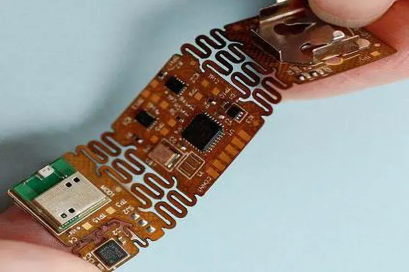
Flexible PCB Circuit Board
Designing PCBs for wearable heart rate monitor bands presents unique challenges that demand meticulous attention to achieve optimal performance, user comfort, and device longevity. These considerations extend beyond traditional PCB manufacturing, encompassing miniaturization, flexibility, and the critical need for robust signal integrity to accurately capture and transmit physiological data. The core objective is to create a compact, durable, and highly reliable electronic foundation that integrates seamlessly into a user's daily life, often in demanding environments.
Miniaturization and Form Factor Wearable devices require PCBs to be exceptionally small and lightweight to maintain user comfort and discreet aesthetics. This necessitates advanced component placement, multi-layer board designs, and the use of micro-vias, significantly increasing routing density and reducing overall board size. According to a report by Mordor Intelligence, the global wearable technology market is projected to grow significantly, driven by the demand for smaller, more efficient devices, directly impacting PCB miniaturization efforts.
Flexibility and Durability Unlike rigid PCBs, heart rate monitor bands often require flexible or rigid-flex PCBs to conform to the body's contours and withstand repeated bending and movement. Material selection, such as polyimide substrates, becomes crucial for maintaining electrical integrity and mechanical robustness over the device's lifespan. The design must account for dynamic stress, preventing trace cracking and delamination, which is a common failure point in poorly designed flexible circuits.
Signal Integrity and Noise Reduction Accurate heart rate monitoring relies on pristine signal integrity from highly sensitive sensors. The PCB design must mitigate electromagnetic interference (EMI), crosstalk, and power supply noise. This involves careful grounding schemes, controlled impedance routing for high-frequency signals, and strategic placement of analog and digital components to prevent interference, ensuring precise data acquisition even in electrically noisy environments.
Power Management and Efficiency Battery life is a paramount concern for wearable devices. The PCB design must prioritize efficient power management, minimizing current leakage and optimizing voltage regulation. This includes selecting low-power components, implementing efficient power distribution networks, and potentially incorporating energy harvesting capabilities, extending operational time between charges and enhancing user experience.
Thermal Management Despite their small size, components on wearable PCBs can generate heat. Effective thermal management is essential to prevent performance degradation and ensure user safety. This involves selecting materials with good thermal conductivity, employing thermal vias, and strategically placing heat-dissipating components. Without proper thermal design, device reliability and longevity can be significantly compromised, leading to premature failure.
Biocompatibility and Environmental Resistance Given direct skin contact, PCB materials and coatings must be biocompatible to prevent skin irritation or allergic reactions. Furthermore, the PCB needs to withstand various environmental factors such as sweat, humidity, and occasional water exposure. Conformal coatings, sealed enclosures, and robust material choices are crucial for long-term reliability and user health.
Material Selection for Optimal Performance and Durability
PCB Raw Materials
Selecting the appropriate materials is paramount in the development of Printed Circuit Boards (PCBs) for wearable heart rate monitor bands, directly influencing the device's performance, durability, and user comfort. Given the intimate contact with skin and constant movement, these PCBs demand materials that offer a unique blend of flexibility, efficient thermal management, and biocompatibility, ensuring both reliable functionality and user safety.
Material Property
Key Consideration for Wearable PCBs
Typical Material Choices & Benefits
Flexibility & Bendability
Essential for conforming to body contours and resisting repeated flexing without signal integrity loss.
Flexible Copper Clad Laminates (FCCL) like Polyimide (PI) or PEN offer excellent flexibility and durability. LCP (Liquid Crystal Polymer) provides high-frequency performance and low moisture absorption.
Thermal Conductivity
Critical for dissipating heat generated by electronic components, preventing overheating and ensuring stable performance.
Materials with good thermal conductivity such as Aluminum (Al) substrates or specialized thermally conductive prepregs help in efficient heat dissipation, enhancing component lifespan and device reliability. Copper layers also contribute significantly to heat spreading.
Biocompatibility
Mandatory for skin-contact devices to prevent irritation, allergic reactions, or long-term health issues.
Medical-grade FR-4 (with appropriate surface finishes), Polyimide, and specific epoxy resins are often chosen. Gold (Au) or Nickel-Gold (Ni/Au) plating on contact pads ensures hypoallergenic properties and corrosion resistance for skin interaction.
Durability & Reliability
Must withstand sweat, impact, abrasion, and environmental factors without compromising electrical performance.
High-Tg (glass transition temperature) FR-4 for rigid sections provides dimensional stability. Conformal coatings (e.g., Parylene, Acrylic, Silicone) offer moisture and chemical resistance. Robust soldermasks and surface finishes (ENIG, OSP) protect exposed copper.
Beyond the primary considerations, other factors like dielectric constant (Dk) and dissipation factor (Df) are crucial for high-frequency signal transmission, particularly in advanced sensor applications. Low Dk/Df materials minimize signal loss, which is vital for accurate heart rate readings. Furthermore, the material's resistance to moisture and chemicals (e.g., sweat, lotions) ensures long-term reliability in real-world usage. Zero One Solution Limited leverages its extensive experience and global supply chain network to source and utilize cutting-edge materials, ensuring our PCB solutions for wearable heart rate monitor bands meet the most stringent performance and durability standards.
Manufacturing Processes: Ensuring Precision and Reliability
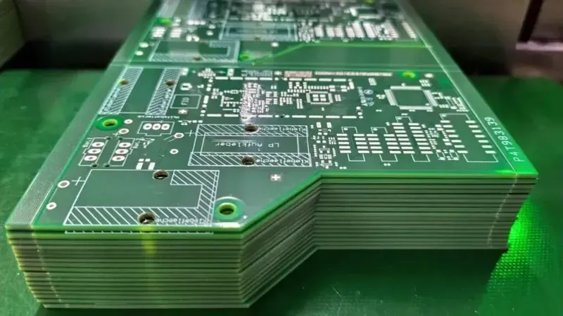
PCB Manufacturing Process
The journey from a conceptual design to a functional wearable heart rate monitor band PCB demands an intricate and highly precise manufacturing process. Each step, from substrate preparation to final testing, is critical to ensuring the reliability, durability, and performance required for these intimate, body-worn devices. For a wearable heart rate monitor, the manufacturing process must account for factors like miniaturization, flexibility, and robust signal integrity under continuous use and environmental stress.
Substrate Preparation and Imaging The process begins with the selection and preparation of the core PCB material, often a flexible polyimide for wearable applications. The substrate is meticulously cleaned, and then a thin layer of copper is laminated onto it. Photolithography is used to transfer the circuit design onto the copper layer. This involves applying a photoresist, exposing it to UV light through a photomask that outlines the circuit pattern, and then developing the resist to reveal the desired copper traces and pads. Precision in this step is paramount for achieving the minute geometries characteristic of wearable PCBs.
Etching and Multi-Layer Lamination Following imaging, unwanted copper is chemically etched away, leaving only the circuit traces. For multi-layer PCBs, which are common in sophisticated wearable devices, individual layers are fabricated separately. These layers are then carefully aligned and laminated together under high temperature and pressure, often with prepreg (fiberglass impregnated with epoxy resin) acting as an insulating adhesive. Accurate registration of layers is crucial to prevent electrical shorts and ensure proper connectivity.
Drilling and Plating Once the layers are laminated, holes are drilled through the PCB using high-precision CNC machines or laser drills. These holes serve as vias (vertical interconnect access) to connect different layers electrically, and as mounting points for components. After drilling, the inner walls of the holes are chemically plated with copper to ensure electrical continuity between layers. This plating process, often involving electroless and electrolytic copper deposition, must be uniform and robust to guarantee signal integrity and long-term reliability.
Solder Mask and Surface Finish Application A solder mask, typically a green polymer layer, is applied over the copper traces to protect them from oxidation, corrosion, and accidental shorting during assembly. Openings are left only for the component pads. After the solder mask, a surface finish is applied to the exposed copper pads. Common finishes for wearable PCBs include Electroless Nickel Immersion Gold (ENIG) or Organic Solderability Preservative (OSP), which protect the copper and ensure excellent solderability for component mounting.
Component Assembly (PCBA) This is where the raw PCB transforms into a functional electronic assembly. Surface Mount Technology (SMT) is primarily used, involving automated pick-and-place machines that precisely position tiny electronic components (like microcontrollers, sensors, and power management ICs) onto the solder paste applied to the pads. The board then passes through a reflow oven, where the solder paste melts and forms robust electrical and mechanical connections. For flexible PCBs, specialized low-temperature solders or flex-specific assembly techniques may be employed to prevent damage.
Testing and Quality Control Rigorous testing is performed at various stages to ensure the PCB meets all design specifications and functional requirements. This includes Automated Optical Inspection (AOI) to check for manufacturing defects like shorts or opens, In-Circuit Testing (ICT) to verify component placement and connectivity, and Functional Testing to simulate real-world operation and confirm the device's performance. Environmental testing, such as temperature and humidity cycling, is also crucial for wearable devices to ensure long-term durability in diverse conditions.
Zero One Solution Limited: Your Partner in PCB Solutions
In the rapidly evolving landscape of wearable health technology, the ability to rapidly prototype and iterate on designs is paramount. Zero One Solution Limited stands as a pioneering force in providing comprehensive PCB solutions, empowering innovators to bring cutting-edge wearable heart rate monitor bands to market with unprecedented speed and precision. Our deep expertise, coupled with a robust one-stop service model, positions us as the ideal partner for your next groundbreaking project.
Rapid Prototyping & Agile Development At the core of our offering is an unmatched capability for rapid prototyping. We understand the critical need for quick turnaround times in R&D, allowing our clients to test, refine, and validate their wearable heart rate monitor band designs efficiently. This agility significantly reduces time-to-market and accelerates innovation cycles.
Comprehensive One-Stop PCBA Services Zero One Solution Limited provides a seamless, integrated approach from PCB design to manufacturing and assembly. This one-stop service eliminates the complexities of managing multiple vendors, ensuring consistent quality, streamlined communication, and optimized project timelines for your wearable heart rate monitor band PCB solutions.
Specialized Expertise in Wearable Technology PCBs With over a decade of experience, we possess specialized knowledge in the unique challenges of wearable PCBs, including miniaturization, flexibility, signal integrity for biometric sensors, and robust material selection. Our team is adept at navigating the intricate requirements of high-performance, low-power wearable devices.
Global Supply Chain and Strategic Locations Headquartered in Shenzhen, China, and with a strategic branch office in Dubai, Zero One Solution Limited leverages a robust global PCBA supply chain. This strategic presence ensures access to the highest quality components and raw materials, competitive pricing, and efficient logistics, providing a significant advantage for our clients worldwide.
Service Aspect
Zero One Solution Limited Advantage
Impact on Wearable PCB Projects
Design for Manufacturability (DFM)
Proactive identification of manufacturing efficiencies and cost-saving opportunities during design phase.
Reduces re-spins and optimizes production costs for heart rate monitor band PCBs.
Quality Assurance & Testing
Rigorous testing protocols (AOI, X-ray, ICT, FCT) ensure high reliability and performance of every PCB.
Minimizes field failures and enhances device longevity for wearable heart rate monitors.
Post-Assembly Support
Ongoing technical support and troubleshooting to ensure optimal product performance and customer satisfaction.
Ensures long-term viability and success of wearable devices.
Case Studies: Successful Wearable Heart Rate Monitor Band Projects
heart rate monitor band project
Zero One Solution Limited's extensive experience in PCB manufacturing is best demonstrated through our successful collaborations on numerous wearable heart rate monitor band projects. Our agility in rapid prototyping and commitment to precision have enabled clients to overcome complex design challenges and bring innovative health monitoring devices to market efficiently. These case studies underscore our capability to deliver tailored, high-performance PCB solutions that meet the stringent demands of the wearable technology sector.
Project Name
Client Challenge
Zero One Solution's Contribution
Key Outcome
Ultra-Slim Fitness Tracker
Miniaturization and high flexibility for a sleek design.
Developed a multi-layer flexible PCB with a thickness of 0.3mm, integrating advanced signal integrity features.
Achieved a 25% reduction in device size while enhancing accuracy and comfort, leading to strong market adoption.
Project Name
Client Challenge
Zero One Solution's Contribution
Key Outcome
Rugged Outdoor HR Monitor
Durability and water resistance for extreme environments.
Engineered PCBs with specialized conformal coatings and robust component mounting techniques to withstand harsh conditions.
Ensured IP68 water and dust resistance, enabling reliable performance in diverse outdoor activities and expanding target markets.
Project Name
Client Challenge
Zero One Solution's Contribution
Key Outcome
Medical-Grade ECG Band
High precision, low noise, and stringent regulatory compliance (ISO 13485).
Designed and manufactured PCBs with optimized analog signal paths and EMI shielding, adhering to medical device quality standards.
Successfully passed rigorous medical certifications, allowing for clinical use and positioning the client as a leader in wearable medical diagnostics.
Project Name
Client Challenge
Zero One Solution's Contribution
Key Outcome
Cost-Optimized Wellness Band
Balancing performance with competitive pricing for mass market.
Implemented intelligent panelization and material selection to reduce manufacturing costs without compromising essential features or reliability.
Enabled the client to achieve a 15% cost saving per unit, facilitating aggressive pricing and significant market share growth.
The Future of PCB Technology in Wearable Health Monitoring
The trajectory of wearable health monitoring is inextricably linked to the relentless innovation in Printed Circuit Board (PCB) technology. As devices become more sophisticated, compact, and user-centric, the underlying PCB infrastructure must evolve to support advanced functionalities, enhanced data processing, and prolonged battery life. This evolution is driven by a demand for seamless integration into daily life, pushing the boundaries of traditional rigid circuit boards towards more dynamic, adaptable, and efficient designs.
Miniaturization and High-Density Interconnect (HDI) The relentless pursuit of smaller, lighter, and less obtrusive wearable devices necessitates extreme miniaturization of PCBs. HDI technology, with its finer lines, smaller vias, and increased routing density, is pivotal. It enables the packing of more components into a reduced footprint, enhancing device capability without compromising wearability. This trend is critical for next-generation smart rings, patches, and embedded sensors, where space is at an absolute premium. According to recent industry reports, the global HDI PCB market is projected to grow significantly, driven largely by the miniaturization demands of consumer electronics and medical devices, underscoring its future importance in wearable health.
Flexible and Stretchable PCBs Rigid PCBs have limitations in conforming to the human body's contours or enduring repeated flexing motions. Flexible PCBs (FPCBs) and the nascent field of stretchable electronics are revolutionary for wearable heart rate monitors. FPCBs allow for designs that bend, fold, and twist, enabling integration into soft materials or irregular shapes, improving comfort and aesthetics. Stretchable PCBs, still largely in R&D, promise unprecedented conformability and durability, resisting strain from body movements and offering truly 'wearable' electronics that feel like fabric. This opens doors for smart textiles and direct skin integration for continuous, imperceptible health monitoring.
Advanced Sensor Integration Future wearable heart rate monitors will integrate a wider array of biosensors beyond just PPG (photoplethysmography). This includes ECG (electrocardiogram), SpO2 (blood oxygen saturation), body temperature, sweat analysis, and even neural activity sensors. PCB technology will need to facilitate the seamless integration of these diverse sensor types, managing complex analog and digital signals, minimizing noise, and ensuring data accuracy. This requires multi-layer PCBs with optimized impedance control and advanced shielding techniques to prevent signal interference from multiple concurrent readings.
PCB Technology Trend
Impact on Wearable Heart Rate Monitors
Key Advantages
Miniaturization & HDI
Enables smaller, more discreet devices; integrates more features in compact designs.
Increased functionality per unit area; reduced device footprint and weight; enhanced aesthetics and comfort for the user in everyday wear.
Flexible & Stretchable PCBs
Allows for ergonomic designs; improves comfort and durability during movement.
Conformity to body contours; enhanced durability against mechanical stress; seamless integration into clothing and accessories; improved user experience.
Advanced Sensor Integration
Facilitates multi-parameter health monitoring; improves diagnostic capabilities.
Comprehensive health insights; early detection of health anomalies; personalized health management and proactive care; expands the utility beyond basic heart rate tracking.
FAQs about Wearable Heart Rate Monitor Band PCBs
Understanding the intricacies of Printed Circuit Boards (PCBs) in wearable heart rate monitor bands is crucial for both developers and end-users. These FAQs address common queries about the design, manufacturing, and application of PCBs in this critical health technology, aiming to demystify the core components that enable reliable heart rate tracking.
What makes a PCB suitable for a wearable heart rate monitor band? A PCB for a wearable heart rate monitor band must possess specific characteristics: extreme miniaturization for form factor, flexibility to conform to the body and withstand movement, high signal integrity for accurate sensor readings, low power consumption to extend battery life, and excellent reliability to endure daily wear and environmental factors. Materials like flexible polyimide and specialized conductive inks are often employed to meet these demanding requirements, ensuring the device is both comfortable and functional for continuous monitoring.
How does Zero One Solution Limited ensure signal integrity in wearable heart rate monitor band PCBs? Zero One Solution Limited employs advanced design and manufacturing techniques to guarantee superior signal integrity. This includes precise impedance control, optimized trace routing to minimize interference (EMI/RFI), careful component placement to reduce noise, and the use of high-frequency compatible materials. Our rigorous testing protocols, including high-speed signal analysis and electromagnetic compatibility (EMC) testing, further validate the integrity of the PCB, ensuring accurate and consistent heart rate data acquisition from the sensor to the processing unit.
What are the common challenges in manufacturing flexible PCBs for wearable devices? Manufacturing flexible PCBs for wearable devices presents unique challenges, primarily due to the delicate nature of flexible substrates and the need for precision. These challenges include achieving consistent trace width and spacing on a flexible base, managing material shrinkage during processing, ensuring reliable component attachment on dynamic surfaces, and maintaining dimensional stability throughout the fabrication process. Specialized handling, precise laser drilling, and advanced lamination techniques are essential to overcome these hurdles and produce high-quality, durable flexible PCBs for wearable applications.
These frequently asked questions highlight the critical role of advanced PCB technology in the efficacy and reliability of wearable heart rate monitors, showcasing the specialized expertise required for their development and production.
In conclusion, the PCB solution is a cornerstone of high-performance wearable heart rate monitor bands. Zero One Solution Limited stands at the forefront, providing comprehensive PCB solutions from design to manufacturing. We empower our clients to innovate and lead in the rapidly evolving wearable technology market. Contact us today to discover how our expertise can bring your wearable project to life. Let Zero One Solution Limited be your trusted partner in creating the next generation of wearable heart rate monitoring technology. Share this article and join the conversation!