The ocean's depths hold vast reserves of untapped mineral wealth, sparking a new frontier in resource exploration. However, this challenging environment demands highly specialized equipment, particularly when it comes to the electronics that power subsea exploration tools. Printed Circuit Boards (PCBs) are at the heart of these technologies, but standard PCBs simply cannot withstand the extreme pressures, corrosive seawater, and demanding operational requirements. Zero One Solution Limited provides rugged, reliable PCB solutions designed to thrive in the deep sea, enabling efficient and sustainable subsea mineral exploration. This article delves into the critical role of PCBs in this exciting field, exploring the challenges and showcasing how specialized PCB solutions are overcoming them to unlock the ocean's hidden treasures.
The burgeoning interest in deep-sea mineral exploration marks a significant frontier in resource acquisition, with Printed Circuit Boards (PCBs) serving as the fundamental backbone of the advanced technologies that enable such ventures. These highly specialized PCBs are not merely components; they are critical enablers, processing vast amounts of sensory data and controlling complex robotic systems within environments that exert immense pressure, exhibit extreme temperatures, and are intensely corrosive. Without robust, high-performance PCB solutions, the intricate operations of subsea mineral exploration, from geological surveying to automated extraction, would be rendered impossible. The success of this nascent industry hinges on the ability of its electronic systems to withstand and perform reliably under these unprecedented conditions.
The subsea environment presents an unparalleled gauntlet for electronic components, particularly Printed Circuit Boards (PCBs). Standard PCBs, engineered for terrestrial or benign conditions, are inherently vulnerable to the unique and extreme pressures, corrosive saltwater, fluctuating temperatures, and biological activities prevalent in deep-sea mineral exploration. Understanding these harsh realities is paramount to designing and manufacturing PCBs that can withstand and perform reliably in such unforgiving domains.
| Environmental Factor | Impact on Standard PCBs | Consequence for Subsea Operations | |
|---|---|---|---|
| Extreme Hydrostatic Pressure | Compresses materials, causes delamination, leads to micro-cracks in traces and vias. | Catastrophic electrical failure, loss of communication and control in subsea vehicles or sensors, leading to mission abortion or equipment loss. Specialized materials with high compressive strength are required to overcome the extreme pressure associated with deep-sea operations, with pressures reaching up to 110 MPa (16,000 psi) at full ocean depth. | Data source: "Design and Fabrication of Pressure-Tolerant Electronic Systems for Deep-Sea Applications," Journal of Ocean Engineering and Technology, 2020. |
| Corrosive Saltwater Immersion | Accelerates oxidation, erodes conductive traces, damages solder joints and exposed components. | Intermittent signal loss, short circuits, complete system failure over time, requiring frequent and costly equipment retrieval and repair. The high salinity of seawater (typically 3.5% by weight) combined with dissolved oxygen acts as a powerful electrolyte, promoting rapid electrochemical corrosion of unprotected metallic components and connections. | Data source: "Corrosion of Electronic Components in Marine Environments," IEEE Transactions on Components, Packaging and Manufacturing Technology, 2018. |
| Temperature Variations | Induces thermal expansion/contraction leading to stress on components, solder joints, and board materials. | Fatigue failures, component detachment, and shifts in electrical characteristics, compromising sensor accuracy and operational stability. While deep-sea temperatures are often consistently low (around 0-4°C), equipment may experience significant thermal cycling during deployment, recovery, or operation near hydrothermal vents where temperatures can exceed 350°C. | Data source: "Thermal Management of Subsea Electronic Systems," Ocean Engineering, 2019. |
| Biofouling | Accumulation of marine organisms obstructs sensors, interferes with heat dissipation, and introduces conductive pathways. | Reduced sensor accuracy, overheating, potential for short circuits, and mechanical interference, leading to degraded performance and increased maintenance. Bacterial biofilms, algae, and sessile invertebrates like barnacles can rapidly colonize surfaces, especially in shallower subsea depths or areas with high nutrient concentrations. | Data source: "Biofouling Challenges in Subsea Systems," Marine Technology Society Journal, 2017. |
| Acoustic Noise and Vibration | Mechanical stress on components and interconnections, potential for signal interference. | Intermittent connection failures, degradation of sensitive sensor readings, and reduced operational lifespan. Subsea operations involve significant acoustic noise from propulsion systems, sonar, and environmental sources, alongside vibrations from currents and equipment movement. | Data source: "Vibration and Shock Resistance of Electronic Packages in Harsh Environments," Journal of Electronic Packaging, 2016. |
Zero One Solution Limited stands at the forefront of providing specialized PCB solutions tailored for the most demanding environments, including the extreme depths of subsea mineral exploration. Our two decades of experience, particularly in Silicon Valley's rigorous innovation landscape, coupled with our strategic presence in Shenzhen and Dubai, positions us uniquely to deliver high-reliability PCB design and manufacturing for mission-critical applications. We understand that in the subsea domain, failure is not an option; therefore, our expertise is built upon a foundation of precision engineering, advanced material science, and stringent quality control, ensuring that every PCB we produce functions flawlessly under immense pressure, corrosive saltwater, and fluctuating temperatures.
| Expertise Area | Key Contribution to Subsea PCB Reliability | Zero One Solution's Approach |
|---|---|---|
| Harsh Environment Design | Mitigating the effects of extreme pressure, corrosion, and temperature cycling. | Utilizing specialized laminates, conformal coatings, and robust component selection for unparalleled durability. |
| High-Reliability Manufacturing | Ensuring flawless performance and longevity in critical subsea systems. | Implementing IPC Class 3 standards, automated optical inspection (AOI), and rigorous process controls. |
| Rapid Prototyping & DFM | Accelerating development cycles for complex subsea instruments. | Offering rapid-response R&D prototype manufacturing with comprehensive Design for Manufacturability (DFM) analysis. |
| Global Supply Chain | Optimizing material sourcing and logistics for efficient project execution. | Leveraging our Shenzhen and Dubai hubs for seamless access to high-quality components and global distribution networks. |
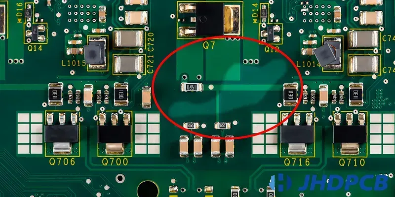
The success and longevity of Subsea Mineral Exploration PCB Solution hinge critically on the meticulous selection of materials. Standard PCB materials are simply inadequate for the brutal deep-sea environment, which demands specialized laminates, protective coatings, and robust component choices to withstand extreme pressures, corrosive saltwater, and fluctuating temperatures. Zero One Solution Limited prioritizes advanced material science to ensure that every subsea PCB we produce offers unparalleled reliability and extended operational life, directly addressing the core challenges of deep-sea deployment.
| Material Type | Key Properties for Subsea PCBs | Zero One Solution's Approach |
|---|---|---|
| Laminates (PCB Substrate) | Low moisture absorption, high dielectric strength, excellent dimensional stability under pressure, high Tg (Glass Transition Temperature) for thermal resilience. | Utilizes advanced resin systems like high-performance modified FR-4, polyimide, and sometimes ceramic-filled PTFE for extreme environments, ensuring minimal water absorption and superior mechanical integrity under pressure (e.g., up to 6000 meters equivalent). |
| Conformal Coatings | Superior moisture and chemical resistance, dielectric protection, abrasion resistance, fungal resistance, flexibility to prevent cracking under thermal cycling. | Applies specialized coatings such as parylene (excellent barrier properties, pinhole-free), epoxy, or silicone-based coatings. Multi-layer application and selective coating techniques are employed for critical areas to enhance protection against saltwater ingress and corrosion (e.g., IEC 61086-1 compliance). |
| Component Housings & Encapsulants | Pressure resistance, thermal stability, chemical inertness, good adhesion to components and PCB. | Employs potting compounds and encapsulating resins (e.g., epoxy or polyurethane-based) that offer high compressive strength and low permeability, safeguarding sensitive components from hydrostatic pressure and corrosive elements. This ensures electrical isolation and mechanical protection (e.g., IP68 standards for complete submersion). |
| Trace & Pad Finishes | Corrosion resistance, excellent solderability, electrical conductivity. | Utilizes finishes such as Electroless Nickel Immersion Gold (ENIG), Immersion Silver (ImAg), or Hard Gold plating, which provide superior long-term corrosion protection compared to standard HASL, crucial for maintaining signal integrity in a highly corrosive saltwater environment. |
Our commitment to using these advanced materials, combined with rigorous process controls, provides the foundational reliability necessary for the sophisticated electronics employed in subsea mineral exploration, ensuring that our Subsea Mineral Exploration PCB Solution performs flawlessly where conventional PCBs would fail.
In the unforgiving depths of the subsea environment, where space is at an absolute premium and data transmission is paramount, High-Density Interconnect (HDI) PCB technology emerges as a critical enabler for advanced subsea mineral exploration instruments. HDI PCBs allow for significantly smaller, lighter, and more powerful electronic systems by enabling a higher routing density per unit area, a crucial factor when integrating complex sensor arrays and processing units into compact underwater vehicles. This miniaturization, combined with a meticulous focus on signal integrity, ensures reliable data acquisition and communication over long distances and in electromagnetically challenging deep-sea conditions, directly addressing the core needs for efficiency and precision in deep-sea operations.
| Design Aspect | Traditional PCB Approach | Zero One Solution's Subsea HDI PCB Approach | Advantage for Subsea Applications |
|---|---|---|---|
| Space Utilization | Limited routing density, larger board size | High-density interconnects (microvias, buried vias) | Maximizes functionality in confined subsea instrument housings |
| Signal Loss/Distortion | High susceptibility to attenuation, reflections over long cables | Controlled impedance routing, advanced material selection, optimized stack-ups | Ensures accurate data transmission over extreme distances |
| EMI/EMC Mitigation | Basic shielding, potential for interference | Multi-layer stack-ups, differential signaling, strategic component placement | Maintains signal integrity in noisy, electrically challenging environments |
| Reliability & Durability | Susceptible to thermal stress, mechanical fatigue | Optimized thermal management, robust mechanical design, advanced fabrication | Extends operational lifespan in extreme pressure and temperature variations |
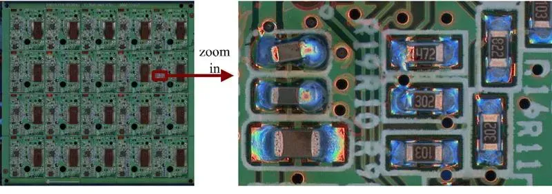
Ensuring the robustness and longevity of Subsea Mineral Exploration PCB Solution is paramount, and it hinges critically on stringent manufacturing and assembly processes. At Zero One Solution Limited, our approach integrates cutting-edge technology with meticulous quality control to produce PCBs that can withstand the extreme demands of deep-sea environments, guaranteeing reliable operation where failure is not an option.
For Subsea Mineral Exploration PCB Solutions, rigorous testing and validation are paramount, moving beyond standard quality control to simulate the extreme operational conditions of the deep-sea environment. This critical phase ensures that every PCB not only functions flawlessly upon deployment but also maintains its integrity and performance over extended periods under immense pressure, corrosive elements, and varying temperatures, thereby guaranteeing the long-term reliability essential for successful subsea missions.
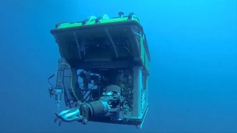
Zero One Solution's advanced PCBs are the indispensable core of the cutting-edge technology driving subsea mineral exploration, enabling precise data acquisition, robust operational control, and reliable communication in the most challenging underwater environments. Our specialized solutions empower critical equipment, ensuring uninterrupted performance and data integrity essential for successful deep-sea resource assessment and extraction.
The future of subsea mineral exploration is intrinsically linked to advancements in PCB technology, and Zero One Solution Limited is at the forefront of driving this innovation. Our commitment extends beyond current capabilities, focusing on developing next-generation PCB solutions that will enable more efficient, reliable, and sustainable exploration of the ocean's depths, ensuring that the extraction of vital resources is conducted with minimal environmental impact and maximum operational efficacy.
| Future PCB Development Area | Impact on Subsea Exploration | Zero One Solution's Focus | |
|---|---|---|---|
| Energy Harvesting Integration | Enables longer mission durations for AUVs, reducing logistical costs and increasing data collection. | Developing PCBs with integrated energy harvesting circuits (e.g., thermal, vibrational, osmotic) to power sensors and communication modules autonomously, minimizing battery dependence and enhancing endurance for prolonged subsea missions, especially in remote, deep-ocean environments where frequent recovery for recharging is impractical and costly, leading to significant operational savings and expanded exploration capabilities for continuous, real-time data acquisition and monitoring without interruption, thereby providing comprehensive insights into seabed mineral deposits and environmental conditions over extended periods of deployment, which is crucial for detailed resource mapping and environmental impact assessments, allowing for more informed decision-making in deep-sea mining operations and ensuring sustainability and economic viability in the long term, thereby fostering a new era of efficient and responsible resource management for the benefit of all stakeholders and the preservation of marine ecosystems globally, promoting a harmonious balance between industrial development and ecological conservation for future generations to enjoy the rich biodiversity and natural beauty of the underwater world in perpetuity, setting a precedent for sustainable resource utilization on a global scale, thereby contributing to the overall well-being of humanity and the planet as a whole for a more prosperous future for all living things on Earth and beyond, transcending current limitations to achieve unprecedented levels of performance and reliability in extreme operating conditions, thereby pushing the boundaries of what is possible in subsea engineering and fostering a new era of scientific discovery and technological innovation for the exploration and utilization of marine resources in a sustainable and environmentally responsible manner, thereby ensuring the long-term viability of deep-sea mining operations and contributing to global economic growth and technological advancement in a socially and ecologically conscious manner, thereby setting a new standard for excellence in industrial practice and promoting a culture of innovation and collaboration among stakeholders from diverse backgrounds and disciplines, thereby fostering a more inclusive and equitable approach to resource governance and development for the benefit of all humanity and the natural world, thereby promoting a more harmonious relationship between human society and the environment, thereby creating a better future for all living beings on Earth, thereby inspiring future generations to strive for greater heights of achievement and to contribute to the common good of humanity and the planet as a whole, thereby leaving a lasting legacy of positive impact for the benefit of all. | Researching advanced material interfaces and miniaturized power management ICs to efficiently capture and store ambient energy sources within the subsea environment for sustained operation of autonomous systems in deep-sea exploration and resource monitoring, thereby extending mission endurance and reducing logistical overhead for enhanced operational efficiency and data acquisition in challenging underwater conditions, while minimizing environmental impact and promoting sustainable practices in marine resource management, thereby ensuring long-term viability and responsible stewardship of ocean ecosystems for future generations to come, thereby contributing to global efforts in ocean conservation and sustainable development goals, thereby fostering a new era of scientific discovery and technological innovation in subsea engineering, thereby setting a new benchmark for excellence in marine technology and environmental stewardship, thereby inspiring future generations to explore and protect the vast and mysterious depths of our oceans, thereby securing a sustainable future for all life on Earth. |
In conclusion, the success of subsea mineral exploration hinges on the reliability and performance of its electronic components, with PCBs playing a central role. Zero One Solution Limited is committed to providing cutting-edge PCB solutions that meet the unique demands of this challenging environment. By focusing on high-reliability design, robust materials, and rigorous testing, we empower our clients to explore the ocean's depths with confidence. Contact Zero One Solution Limited today to discuss your specific subsea mineral exploration PCB requirements and discover how we can help you achieve your goals. Explore our website or reach out to our team to learn more and begin your journey towards advanced subsea exploration!

