
In the fast-evolving world of automotive lighting, thermal efficiency is not just a feature—it is a safety requirement. Aluminum Core PCBs (MCPCBs) provide the necessary heat dissipation for high-power LEDs, but they require precision design. This guide breaks down the essential DFM rules to ensure your designs survive the rigors of the road.
Understanding the Aluminum Core PCB Stackup
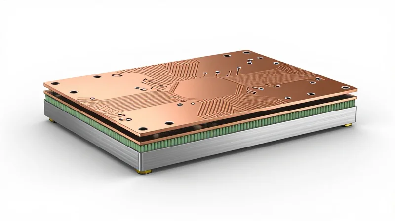
Core Components of the MCPCB Stackup
An Aluminum Core PCB, or Metal Core Printed Circuit Board (MCPCB), is engineered specifically to facilitate high-efficiency thermal management. Unlike standard FR-4 substrates, the MCPCB architecture replaces the center glass-epoxy layer with a thermally conductive aluminum alloy base. This base serves as both a structural foundation and an integrated heat spreader, drawing thermal energy away from high-power LEDs utilized in modern automotive lighting systems.
| Layer | Function | Material |
|---|---|---|
| Circuit Layer | Conducts current and signals | Copper Foil |
| Dielectric Layer | Electrical insulation & thermal transfer | Thermally Conductive Prepreg |
| Base Layer | Structural integrity & heat sink | Aluminum Alloy |
Thermal Dielectric Performance
The dielectric layer is the critical interface between the copper circuit and the aluminum base. In automotive applications, where vibration and thermal cycling are constant, this layer must exhibit high thermal conductivity (typically 1.0 to 3.0 W/mK) while maintaining strict dielectric breakdown strength. Selecting the correct dielectric is paramount to prevent short-circuits caused by thermal expansion mismatches during extreme temperature swings.
Frequently Asked Questions
- Why is the dielectric layer thinner than in FR-4 PCBs?
The dielectric must be as thin as possible to minimize thermal resistance, as thicker layers impede heat transfer from the LED junctions to the aluminum core. - How does the aluminum base affect PCB mounting?
The aluminum base is conductive; therefore, designers must ensure appropriate creepage and clearance distances are maintained between circuitry and the chassis to prevent electrical arcing.
Optimizing Dielectric Layer Thickness
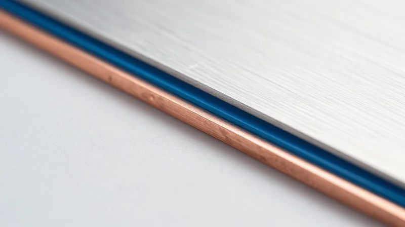
The Thermal-Electrical Paradox
The dielectric layer acts as the interface between the copper circuit and the aluminum substrate. Increasing the thickness of this layer enhances dielectric withstand voltage (DWV) and isolation, but simultaneously introduces higher thermal resistance (Rth). For automotive lighting, where power densities are rising, designers must select the thinnest possible dielectric that meets the specific breakdown voltage requirements of the vehicle's electrical architecture.
Comparison of Dielectric Thickness Impact
| Dielectric Thickness (µm) | Thermal Performance | Isolation Capability | Recommended Application |
|---|---|---|---|
| 50 - 75 | Excellent (Low Rth) | Moderate | High-power headlight modules |
| 100 - 150 | Good | High | Standard signal lighting |
| 200+ | Poor (High Rth) | Very High | High-voltage EV powertrain lighting |
Design Guidelines for Automotive Reliability
- How does dielectric thermal conductivity affect layer thickness selection?
Materials with higher thermal conductivity (e.g., ceramic-filled polymers) allow for thicker dielectric layers while maintaining lower total thermal resistance, providing a safety margin for isolation without sacrificing heat dissipation. - What are the common failure modes linked to improper thickness?
Dielectrics that are too thin risk partial discharge and insulation breakdown during voltage surges, whereas overly thick layers can lead to excessive junction temperatures and premature LED degradation. - Is a uniform thickness always required?
No, while uniform thickness simplifies manufacturing, local variations or selective thinning can be used near high-heat zones, provided the PCB manufacturer can maintain precise control over the lamination pressure.
To achieve optimal reliability, designers should prioritize a thermal-mechanical simulation early in the layout phase. This ensures the dielectric thickness is sufficient for automotive transient pulse requirements (e.g., ISO 7637-2 standards) while keeping the LED junction temperature well below the manufacturer's recommended limit.
Copper Weight Requirements for High-Current Circuits
Determining Copper Weight for High-Current Thermal Management
For automotive LED applications, the copper circuit layer must balance current-carrying capacity with manufacturing precision. In high-power lighting circuits, thinner copper increases thermal impedance, while excessive thickness can hinder the etching resolution of fine-pitch pads required for modern LED packages. Designers should utilize IPC-2152 standards rather than legacy IPC-2221 formulas to accurately calculate the permissible temperature rise for copper traces on insulated metal substrates.
Copper Weight Selection Guidelines
| Copper Weight (oz) | Thickness (mm) | Primary Application | Thermal Performance |
|---|---|---|---|
| 1.0 oz | 0.035 mm | Low-current control/sensing | Moderate |
| 2.0 oz | 0.070 mm | Standard automotive LED strings | High |
| 3.0 oz+ | 0.105 mm+ | High-power headlight modules | Superior |
Technical FAQ: Copper Weights and Reliability
- How does copper thickness affect etching?
As copper thickness increases, the etching factor becomes more significant. For 3oz copper, designers must account for wider trace gaps to accommodate undercut and ensure long-term dielectric integrity. - Is thicker copper always better for heat dissipation?
While thicker copper reduces electrical resistance and heat generation, it also increases the thermal mass. In automotive lighting, balancing trace cross-sectional area with the thermal conductivity of the dielectric layer is vital for overall reliability. - What is the recommended standard for high-brightness LEDs?
Most high-reliability automotive designs standardize on 2oz (70µm) copper to provide a robust balance between thermal conductivity and manufacturing cost-efficiency.
Strategic Thermal Via Placement
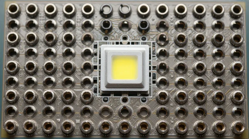
Maximizing Heat Path Efficiency
To achieve optimal thermal management, thermal vias must be strategically positioned directly beneath the LED thermal pad. The primary goal is to minimize the path length through the dielectric layer, which serves as the most significant thermal bottleneck. By employing a high-density array of copper-plated vias, designers can provide a low-resistance path that sinks heat directly into the aluminum base plate, effectively preventing junction temperature excursions that degrade phosphor and semiconductor longevity.
Via-in-Pad vs. Peripheral Stitching
| Method | Thermal Performance | Manufacturing Complexity | Reliability Impact |
|---|---|---|---|
| Via-in-Pad | Highest | High (requires planarization) | Requires secondary process |
| Peripheral Stitching | Moderate | Low | Standard SMT assembly |
Best Practices and Design Rules
- How should thermal vias be processed for automotive standards?
Always specify copper-filled and capped vias (IPC-4761 Type VII) to prevent solder wicking and ensure a flat, stable mounting surface for the LED package. - What is the recommended pitch for thermal stitching?
Maintain a pitch between 0.8mm and 1.2mm to balance thermal conductivity with structural integrity, ensuring that too many holes do not compromise the mechanical strength of the dielectric interface. - How do you avoid dielectric degradation during drilling?
Utilize precision laser drilling or controlled-depth mechanical drilling to prevent micro-cracking of the thermal dielectric layer, which could otherwise lead to premature dielectric breakdown.
For high-reliability automotive environments, it is imperative to verify that the plating thickness within the via barrels meets at least 25 micrometers. This ensures the structural integrity of the thermal path under thermal cycling, preventing the delamination of the copper-aluminum interface over years of extreme temperature fluctuations.
Material Selection and Tg Ratings
In high-reliability automotive lighting, the dielectric layer is the single most critical interface between the LED heat source and the aluminum base plate. For these applications, standard FR-4 epoxies are insufficient; designers must specify thermally conductive, high-glass transition temperature (Tg) prepregs. The glass transition temperature represents the threshold where the polymer matrix transitions from a rigid, glassy state to a flexible, rubbery state. Operating near or above this threshold triggers thermal expansion mismatches, leading to delamination, cracked dielectric layers, or fractured solder joints.
Comparative Performance of Dielectric Systems
| Material Property | Standard Epoxy | High-Performance Ceramic-Filled | Automotive Reliability Impact |
|---|---|---|---|
| Tg (Glass Transition) | 130-150°C | 170-190°C | Prevents Z-axis expansion at LED heat peaks. |
| Thermal Conductivity | 1.0-2.0 W/mK | 3.0-8.0 W/mK | Reduces junction temperature (Tj). |
| Breakdown Voltage | 3kV - 5kV | 4kV - 6kV | Ensures isolation under high-voltage surges. |
Strategic Material Selection Guidelines
For automotive headlamps and exterior lighting, we recommend a Tg of at least 170°C. Furthermore, the dielectric must incorporate spherical alumina or boron nitride fillers to maximize thermal conductivity while maintaining high dielectric strength. Designers should verify that the Coefficient of Thermal Expansion (CTE) of the dielectric is closely matched to the aluminum base to minimize stress on the bonded interface during rapid thermal cycling.
Frequently Asked Questions
- Why is a high Tg rating necessary if the ambient temperature is lower?
Automotive environments involve significant thermal cycling. A high Tg ensures the material remains in a stable elastic state even during transient heat spikes, preventing long-term fatigue in the copper-dielectric interface. - Does higher filler content negatively impact PCB fabrication?
Extremely high filler concentrations can increase material hardness and drill wear. Engineers must balance thermal requirements with manufacturability by selecting optimized filler dispersion grades that allow for standard mechanical drilling processes.
Design for Manufacturing: Routing and Clearances
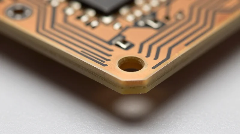
Edge Clearance Requirements
The primary failure mode in aluminum core PCBs is dielectric breakdown at the periphery where copper layers meet the metal substrate. To maintain electrical isolation, copper features must be set back from the edge of the aluminum core. Standard industry practice requires a minimum clearance of 1.0mm to 1.5mm from the conductive path to the mechanical edge of the aluminum base to account for mechanical milling tolerances and potential burr formation during fabrication.
Routing and Trace Geometry
Routing strategies on MCPCBs must prioritize the limitation of capacitive coupling between the copper circuit layer and the aluminum ground plane. Tight radius corners should be avoided in high-voltage segments to mitigate electric field concentration. For automotive lighting, maintaining uniform trace widths is essential to ensure consistent thermal distribution and avoid localized hot spots that could compromise the thin dielectric layer.
| Parameter | Recommended Minimum | Automotive Rationale |
|---|---|---|
| Edge Clearance | 1.25 mm | Prevents HV arcing and edge-burr shorting |
| Internal Cutouts | 1.00 mm | Maintains dielectric integrity at thermal apertures |
| Trace to Edge | 1.50 mm | Safety margin for vibration-induced flexing |
Frequently Asked Questions
- Why is a larger clearance required for MCPCBs compared to standard FR4?
The metal core acts as a reference ground plane. Insufficient clearance increases the risk of conductive pathways forming between the copper traces and the exposed metal edge, especially in environments with high humidity or vibration. - How does routing affect dielectric lifespan?
Sharp trace angles create field concentrations that accelerate dielectric aging through partial discharge, potentially leading to localized carbonization and eventual short-circuiting under extreme thermal cycling.
Adhering to Automotive Quality Standards
Integrating IATF 16949 and AEC-Q Standards into PCB Design
Achieving reliability in automotive lighting demands more than just thermal management; it requires a systematic adherence to IATF 16949 quality management frameworks and AEC-Q100/101 validation protocols. Designers must move beyond functional performance to focus on deterministic failure prevention by standardizing documentation, traceability, and stress-testing methodologies at the layout stage.
| Standard | Primary Focus | PCB Design Impact |
|---|---|---|
| IATF 16949 | Quality Management | Process control, traceability, and risk analysis. |
| AEC-Q100 | IC Reliability | Thermal cycling limits and humidity resistance. |
| AEC-Q101 | Discrete Components | LED driver and transient voltage protection. |
Key Compliance Strategies for Metal Core PCBs
- Does IATF 16949 influence component placement?
Yes, it mandates strict documentation of clearance paths to prevent creepage-related failures, necessitating a formal Design Failure Mode and Effects Analysis (DFMEA) during the schematic and layout phase. - How is AEC-Q100 verified in DFM?
Verification involves ensuring that thermal interface materials (TIM) and dielectrics maintain mechanical integrity during thermal shock tests, preventing delamination at the core-to-insulator interface. - Why is traceability essential for automotive PCBs?
Traceability ensures that every layer of the aluminum core stack-up can be audited against its material specification sheet (e.g., thermal expansion coefficients) to confirm compliance with extreme climate performance requirements.
To align with these standards, designers must implement a 'zero-defect' mindset. This involves validating that the dielectric layer withstands high-voltage isolation tests post-assembly and that the copper trace weights are optimized for both current density and fatigue resistance. By strictly mapping PCB design parameters to these automotive benchmarks, developers significantly reduce the risk of field recalls and enhance the lifespan of critical lighting modules.
Common Pitfalls and How to Avoid Them
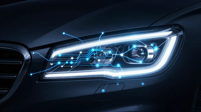
Reliability in automotive LED lighting systems is often compromised by oversights in the PCB layout phase. By preemptively addressing common design pitfalls, engineers can significantly reduce the risk of thermal runaway, dielectric breakdown, and mechanical fatigue under harsh environmental conditions.
Frequent DFM Pitfalls in Metal Core PCBs
| Common Pitfall | Resulting Failure | Prevention Strategy |
|---|---|---|
| Inadequate edge clearance | Short-circuit to core | Ensure 1.0mm minimum routing buffer |
| Thermal via starvation | LED junction overheating | Increase via density in high-wattage zones |
| Excessive dielectric thickness | Increased thermal resistance | Select optimal 50-100um thickness for heat path |
| Unbalanced copper weight | PCB warping/bowing | Specify symmetrical stackups across the core |
Key Questions for Reliability Assessment
- Why does dielectric creepage matter at the edges?
Aluminum core edges are often rough from the cutting process; failing to pull back copper planes ensures the conductive layer does not bridge to the metallic substrate under high-humidity or vibration cycles. - How do I prevent thermal fatigue of solder joints?
Ensure that the Coefficient of Thermal Expansion (CTE) of the dielectric layer is closely matched to the aluminum base; otherwise, differential expansion will cause solder joint cracking during thermal cycling. - Is via filling necessary for automotive LED drivers?
Yes, non-filled vias can trap corrosive flux residues or lead to solder wicking away from the component pads, creating weak electrical connections prone to vibration-induced failure.
Best Practices for Implementation
To ensure long-term performance, enforce strict design rules regarding copper balancing and dielectric selection. Implementing a comprehensive DFM audit before fabrication allows for the identification of potential thermal bottlenecks. Always perform FEA (Finite Element Analysis) on high-power lighting modules to validate that the chosen dielectric conductivity effectively dissipates heat from the LED junction to the aluminum base without introducing localized mechanical stress points.
Successfully engineering automotive-grade aluminum core PCBs requires a meticulous balance of thermal physics and manufacturing reality. By adhering to these DFM best practices, you can maximize thermal performance and reliability. Ready to optimize your next project? Contact our engineering team today for a comprehensive design review.
