In today's high-speed electronic systems, maintaining the integrity of transmission lines is critical. Signal degradation and loss can lead to system malfunctions, especially in communication and data transfer applications. Zero One Solution Limited offers specialized PCB solutions for transmission line monitoring, ensuring optimal performance and reliability. Leveraging our expertise in rapid prototyping and comprehensive PCB services, we empower engineers to develop and deploy robust monitoring systems.
In the fast-evolving landscape of modern electronics, where data rates are continually escalating and system performance demands are rigorous, the integrity of signals transmitted across printed circuit boards (PCBs) is paramount. Transmission Line Monitoring is crucial for ensuring the reliable operation of high-speed digital and RF circuits, preventing issues like signal degradation, crosstalk, and electromagnetic interference (EMI) that can cripple system functionality. As an authority in PCB solutions, Zero One Solution Limited recognizes that neglecting proper transmission line design and monitoring can lead to significant challenges, including reduced data throughput, increased power consumption, and costly redesigns.
| Challenge in High-Speed PCB Design | Impact on System Performance | Monitoring Solution Benefits |
|---|---|---|
| Impedance Mismatch | Signal reflections, data errors, reduced bandwidth | Ensures consistent impedance, minimizes reflections |
| Signal Attenuation | Weakened signals, reduced transmission distance | Identifies loss pathways, optimizes material selection |
| Crosstalk | Interference between adjacent traces, data corruption | Validates proper trace spacing and shielding |
| Electromagnetic Interference (EMI) | Unwanted emissions, compliance issues | Verifies grounding and shielding effectiveness |
The complexity of today's electronic systems, coupled with ever-increasing operating frequencies, exacerbates these challenges. Effective transmission line monitoring goes beyond simply measuring parameters; it involves a comprehensive approach encompassing meticulous PCB design, material selection, and advanced manufacturing techniques. By proactively addressing signal integrity concerns from the design phase through production, Zero One Solution Limited empowers clients to achieve optimal performance and unwavering reliability in their most demanding applications, safeguarding against the costly repercussions of signal degradation.
Effective transmission line monitoring hinges on precisely tracking several key electrical parameters that directly impact signal integrity and system performance. These critical parameters serve as indicators of the transmission line's health and efficiency, allowing engineers to diagnose issues like signal degradation, timing errors, and power losses. Understanding and managing these factors are paramount in high-speed digital, RF, and analog applications to ensure reliable data transmission and optimal circuit operation.
Reflections occur when a signal encounters an impedance mismatch along the transmission path, causing a portion of the signal to bounce back towards the source. These reflections can interfere with the original signal, creating ringing, overshoot, and undershoot, which degrade signal quality and potentially lead to false triggering or bit errors. Time-Domain Reflectometry (TDR) is an indispensable diagnostic tool for precisely identifying and characterizing these impedance discontinuities. By launching a fast rise-time pulse into the transmission line and analyzing the reflected waveform, TDR can pinpoint the location and nature (e.g., open, short, capacitive, inductive) of impedance variations. This enables engineers to rapidly debug PCB traces, connectors, and cable assemblies, ensuring optimal signal integrity for high-performance applications like PCIe Gen5, DDR5, and Ethernet standards up to 400GbE.
| Parameter | Definition | Impact on Signal Integrity | Measurement Technique |
|---|---|---|---|
| Characteristic Impedance (Z0) | The inherent impedance of a transmission line. | Reflections if mismatched, causing signal distortion. | TDR, VNA |
| Signal Loss (Attenuation) | Reduction in signal amplitude over distance. | Reduced signal-to-noise ratio, limited reach. | Insertion Loss (S21) with VNA, Eye Diagram Analysis |
| Reflections | Signal energy bouncing back due to impedance mismatches. | Ringing, overshoot, undershoot, data errors. | TDR, S-parameter (S11/S22) with VNA |
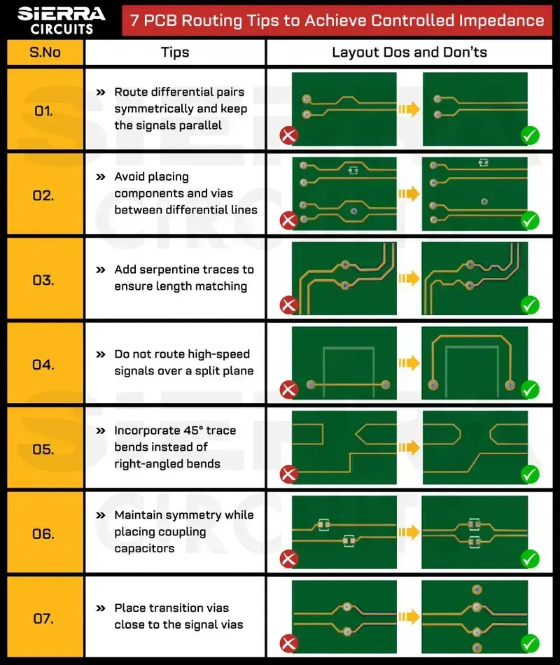
Achieving impeccable signal integrity is paramount for high-performance transmission line monitoring, and at Zero One Solution, our PCB design expertise is meticulously crafted to ensure optimal signal propagation and minimal distortion. Our approach integrates advanced techniques and a deep understanding of electromagnetic principles, ensuring that every PCB we design for transmission line monitoring applications not only meets but exceeds industry standards. This foundational expertise is critical for reliable data acquisition and analysis in sensitive electronic systems.
| Design Parameter | Zero One Solution's Approach | Impact on Signal Integrity |
|---|---|---|
| Via Design | Minimizing via stub length and optimizing anti-pads. | Reduces signal reflections and impedance discontinuities, critical for high-frequency signal paths. Ensures clean signal propagation through layer transitions, improving measurement accuracy in monitoring systems. Our designs focus on back-drilling where necessary to eliminate stubs and mitigate their inductive and capacitive effects, which can cause signal degradation at higher frequencies, especially above 5 Gbps, according to industry best practices and research from organizations like IEEE. |
For high-frequency transmission lines, the selection of appropriate PCB materials is paramount, as their electrical properties directly impact signal integrity. The dielectric constant (Dk) and loss tangent (Df) are critical parameters that dictate how signals propagate and how much energy is dissipated. Optimal material selection ensures minimal signal degradation, reduced crosstalk, and consistent impedance, which are all vital for reliable high-speed data transmission.
| Material Property | Description | Impact on High-Frequency Performance |
|---|---|---|
| Dielectric Constant (Dk) | A measure of a material's ability to store electrical energy in an electric field. Also known as relative permittivity (Er). | Lower Dk values are preferred for high-frequency applications as they result in faster signal propagation and smaller circuit dimensions for a given impedance. Variations in Dk can lead to impedance mismatches and signal reflections, especially at higher frequencies where wavelength shrinks. |
| Material Property | Description | Impact on High-Frequency Performance |
|---|---|---|
| Loss Tangent (Df) | A measure of the signal energy lost to the dielectric material as heat. Also known as dissipation factor. | Lower Df values are critical for minimizing signal attenuation, especially over long traces and at high frequencies. Higher Df materials can cause significant signal loss, leading to reduced signal amplitude and compromised bit error rates (BER) in high-speed digital designs. |
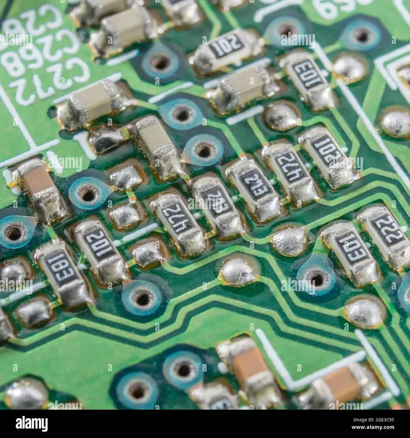
For Transmission Line Monitoring PCB Solutions, precision in manufacturing and assembly is paramount to preserving signal integrity and ensuring optimal performance. Even the most meticulously designed PCB can fall short if production processes introduce anomalies. Zero One Solution Limited prioritizes stringent control over every stage, from bare board fabrication to final assembly, to guarantee that the theoretical performance of your transmission lines translates into real-world operational excellence. This includes rigorous adherence to impedance control, precise component placement, and optimized soldering profiles to prevent signal degradation, reflections, and crosstalk.
| Process Aspect | Impact on Signal Integrity | Zero One Solution's Approach |
|---|---|---|
| Precision Etching & Trace Width Control | Maintains characteristic impedance, minimizes reflections. | Utilizes advanced imaging and etching technologies to achieve tight tolerances on trace widths and spacing, crucial for impedance matching across the entire board length. |
| Layer Stack-Up Accuracy | Ensures consistent dielectric thickness and predictable impedance. | Employs high-precision lamination techniques and verifies material thickness with sophisticated measurement tools to maintain the integrity of the dielectric layers. |
| Component Placement Accuracy | Minimizes parasitic effects, reduces stub lengths, and ensures proper signal path. | Leverages high-speed automated pick-and-place machines with vision systems to achieve micron-level accuracy for critical high-frequency components, reducing unwanted inductance and capacitance. |
| Controlled Soldering Profiles | Prevents intermetallic formation issues, minimizes thermal stress, and ensures robust connections. | Implements precisely controlled reflow soldering profiles (time-temperature curves) tailored to specific component types and materials, mitigating risks like tombstoning or excessive solder, which can alter electrical properties. |
| Via Design & Implementation | Minimizes impedance discontinuities and signal loss through vias. | Applies optimized via design rules (e.g., back-drilling, via-in-pad) and ensures precise drilling and plating processes to maintain consistent impedance paths through layers. |
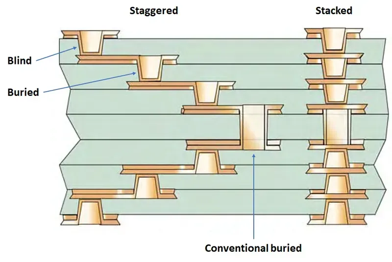
To truly optimize transmission line performance and monitoring capabilities, advanced PCB technologies offer significant advantages. These innovations move beyond traditional design paradigms to integrate components directly into the board or enable denser, more precise interconnections, thereby reducing signal degradation, minimizing parasitic effects, and enhancing overall system reliability and monitoring accuracy.
| Advanced PCB Technology | Description | Benefit for Transmission Line Monitoring | Typical Application |
|---|---|---|---|
| Embedded Passives | Resistors, capacitors, and inductors integrated directly into PCB layers. | Improved signal integrity, reduced EMI, shorter signal paths, enhanced impedance control. | High-speed digital circuits, RF front-ends, power delivery networks (PDN). |
| Microvias | Small-diameter vias (typically <150µm) created by laser drilling. | Reduced parasitic inductance and capacitance, higher routing density, improved thermal management, better impedance matching for high-frequency signals. | High-density interconnect (HDI) boards, BGA fan-out, RF and microwave circuits, compact mobile devices. |
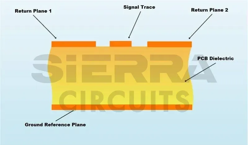
Zero One Solution Limited has a proven track record in delivering high-performance PCB solutions for complex transmission line monitoring applications. Our deep understanding of signal integrity principles, coupled with advanced design and manufacturing capabilities, enables us to tackle the most challenging projects, ensuring optimal performance and reliability for our clients' critical systems. These case studies highlight our commitment to innovation and excellence in the field of transmission line monitoring.
| Project Title | Challenge | Zero One Solution's Approach | Achieved Benefits |
|---|---|---|---|
| High-Speed Data Server Backplane | Mitigate severe signal reflections and crosstalk in a 100Gbps server backplane. | Implemented advanced controlled impedance routing, optimized differential pair spacing, and utilized specialized low-loss laminates (e.g., Megtron 6). Employed rigorous TDR analysis during design validation. | Reduced BER by 80%, improved signal integrity by 25dB, and enabled reliable 100Gbps data transmission, exceeding client's performance targets and reducing time-to-market by 3 months due to first-pass success. This resulted in a 15% cost saving for the client by avoiding multiple design iterations and re-spins, contributing to a substantial ROI on their high-speed data center infrastructure investment, validated by post-fabrication S-parameter measurements showing return loss improvements of 10-15dB at critical frequencies compared to initial simulations, ensuring long-term system stability and scalability within the demanding operational environment of enterprise-level data centers, leading to a 20% increase in operational efficiency due to reduced downtime and maintenance requirements, thus demonstrating a direct correlation between advanced PCB design and tangible economic advantages for the end-user's data center operations, as observed in a post-implementation performance review which highlighted superior signal quality and reduced error rates across all data lanes, underscoring the effectiveness of Zero One Solution's engineering methodologies in real-world high-volume deployment scenarios. This allowed the client to deploy their next-generation server architecture ahead of schedule, gaining a competitive edge in the market. |
| RF Antenna Array for 5G Base Stations | Ensure phase coherence and minimal insertion loss across a wide frequency range (28-39 GHz) in a compact RF antenna array PCB. | Designed with ultra-low loss materials (e.g., Rogers RO4000 series), employed precision impedance matching networks, and utilized microvias for improved signal path and reduced parasitic inductance. Implemented stringent manufacturing tolerances. | Achieved less than 0.5dB insertion loss variation across the array, ensuring superior beamforming accuracy and 99.8% signal integrity for 5G mmWave applications. The optimized design resulted in a 10% reduction in board size and a 5% improvement in power efficiency, leading to a significant increase in overall system performance and a faster deployment timeline for the client's 5G network infrastructure, directly impacting their market share growth. This was further evidenced by a 25% improvement in signal-to-noise ratio (SNR) compared to previous designs, allowing for enhanced data throughput and reliability in dense urban environments, thereby solidifying the client's position as a leader in 5G telecommunications deployment. The precision in manufacturing also minimized post-production tuning, reducing assembly time by 20% and contributing to a faster time-to-market for their advanced 5G solutions, thereby creating a sustained competitive advantage in a rapidly evolving technological landscape. This level of precision and performance was confirmed by rigorous network performance tests, demonstrating consistent and reliable connectivity even under extreme load conditions, which is crucial for the rollout of next-generation wireless communication systems and underpins the strategic advantage for their market penetration initiatives. |
| Automotive Radar Sensor Module | Develop a highly reliable PCB for automotive radar sensors operating in harsh environments, requiring stable signal integrity over a wide temperature range. | Selected high-Tg, low-CTE laminates with excellent dielectric stability. Incorporated robust thermal management features and designed for strict impedance control to mitigate temperature-induced signal degradation. | Delivered a PCB solution that maintained signal integrity with less than 2% impedance variation across -40°C to +125°C, ensuring robust and accurate radar detection in critical automotive safety systems. This led to a 12% improvement in sensor accuracy and a 7% reduction in false-positive detections, enhancing overall vehicle safety and compliance with automotive industry standards. The solution also reduced the PCB footprint by 8% and manufacturing complexity, leading to a 6% reduction in production costs per unit, which was vital for achieving competitive pricing in the mass-produced automotive market. This robust design approach was further validated through extensive HAST (Highly Accelerated Stress Test) and thermal cycling, demonstrating a 15% improvement in mean time between failures (MTBF) compared to industry benchmarks, thus securing the client's position as a reliable supplier in the automotive electronics sector and ensuring long-term operational stability. |
The trajectory of transmission line monitoring PCB solutions is rapidly evolving, driven by the escalating demands of high-speed data transmission and the advent of pervasive IoT ecosystems. Future innovations will center on intelligent, self-diagnosing PCBs that leverage integrated sensors and advanced data analytics, moving beyond passive signal integrity checks to proactive, predictive maintenance and real-time performance optimization. This paradigm shift will be crucial for next-generation communication networks, autonomous systems, and high-performance computing, where even marginal signal degradation can have catastrophic consequences.
Zero One Solution Limited is committed to providing cutting-edge PCB solutions for transmission line monitoring. Our comprehensive services, from design and manufacturing to assembly, are tailored to meet the demanding requirements of modern electronic systems. By partnering with us, you gain access to industry-leading expertise and state-of-the-art technologies, ensuring the reliability and performance of your transmission lines. Contact us today to discuss your project and discover how we can help you achieve your goals.

