In our daily lives, from smartphones to advanced medical equipment, electronic components are indispensable. Among them, the FET transistor, or Field Effect Transistor, plays a crucial role. This article will dive deep into the workings of FET transistors, offering a clear understanding of their importance and applications. We'll cover everything from their basic function to their various types and uses, demystifying this fundamental piece of technology.
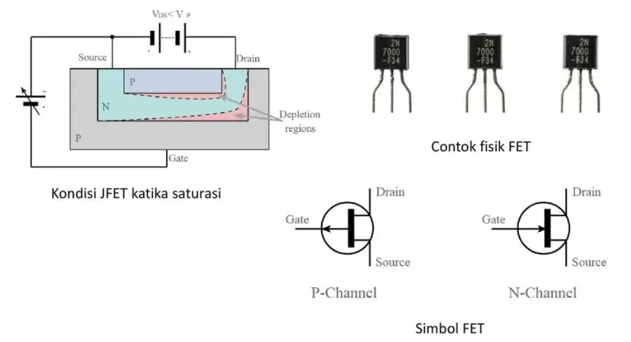
Field-Effect Transistors (FETs) are a cornerstone of modern electronics, acting as voltage-controlled switches or amplifiers. At their core, FETs leverage an electric field to modulate current flow between two terminals—the source and the drain—a mechanism distinctly different from current-controlled devices like bipolar junction transistors (BJTs).
The operation of a FET is governed by three key terminals: the source, which serves as the origin of charge carriers; the drain, where these charge carriers exit the device; and the gate, which is used to apply an electric field. This electric field, controlled by the voltage applied to the gate, alters the conductivity of the channel between the source and drain. The absence of current flow into the gate makes FETs ideal for high impedance applications.
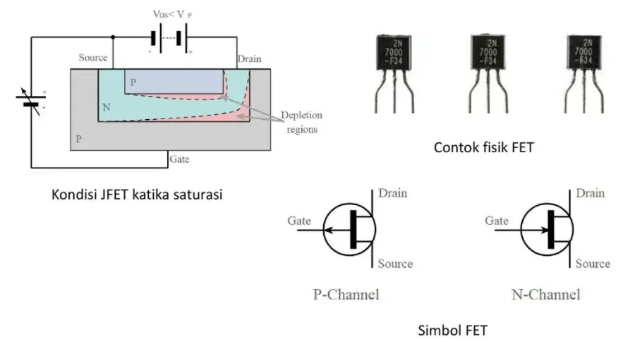
Field-Effect Transistors (FETs) leverage an electric field to modulate current flow, offering a distinct control mechanism compared to traditional bipolar junction transistors (BJTs). The core principle lies in the gate terminal's ability to influence the conductivity of a channel between the source and drain terminals. By applying a voltage to the gate, the electric field either enhances or depletes the charge carriers in this channel, thereby controlling the current that can pass through the transistor. This field-based control makes FETs highly efficient and versatile for various electronic applications.
The operation of a FET revolves around the electric field's effect on a semiconductor channel. When a voltage is applied to the gate terminal, it creates an electric field that penetrates into the channel. This electric field can either attract or repel charge carriers (electrons or holes) depending on the type of FET and the polarity of the applied gate voltage. The modulation of charge carriers directly affects the channel's conductivity, thus controlling the current flow between the source and drain.
Unlike BJTs, which rely on current injection to control output current, FETs use a voltage to create an electric field, allowing for higher input impedance. This distinction is crucial in many circuit applications, as it reduces the load on the driving circuit and leads to more efficient signal processing. This voltage-controlled nature of FETs results in less power consumption and higher switching speeds compared to current-controlled BJTs, making them a preferred choice in many electronic designs.
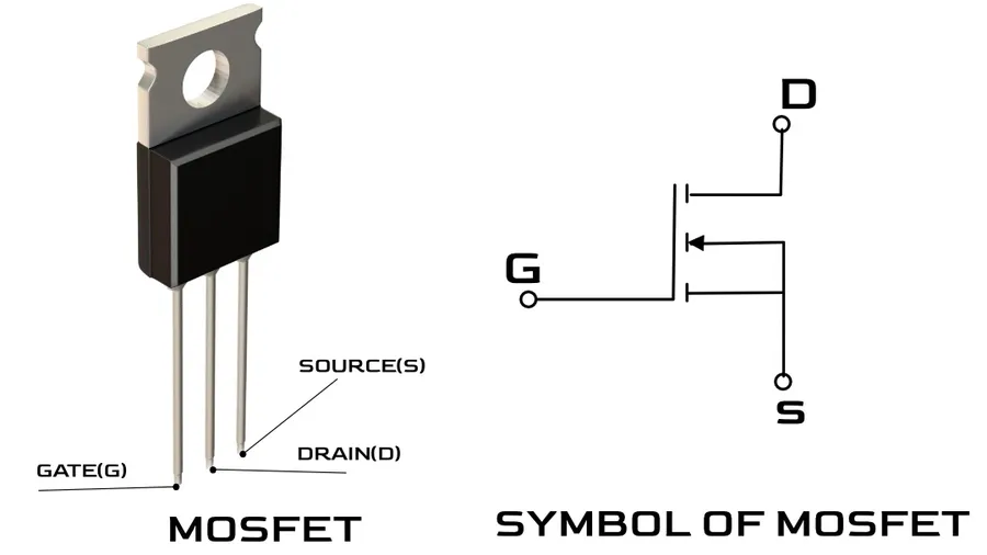
Field-Effect Transistors (FETs) are broadly categorized into two primary types: Junction Field-Effect Transistors (JFETs) and Metal-Oxide-Semiconductor Field-Effect Transistors (MOSFETs). These differ significantly in their structure, operational characteristics, and typical applications. Both JFETs and MOSFETs utilize an electric field to control current flow, but they achieve this control through different physical mechanisms.
| Feature | JFET | MOSFET |
|---|---|---|
| Structure | Semiconductor junction forms the gate | Metal-Oxide-Semiconductor structure forms the gate |
| Gate Isolation | Reverse biased p-n junction | Insulating layer (oxide) separates gate from channel |
| Input Impedance | High, but lower than MOSFET | Extremely high due to gate insulation |
| Control Mechanism | Varying the depletion region width to modulate channel conductivity | Accumulating or depleting charge carriers in channel via the gate voltage |
| Typical Applications | Amplifiers, analog switches | Digital logic, power switching, memory |
| Polarity | Typically operates with a reverse biased gate-source junction | Operates with a gate voltage controlling a conductive channel |
JFETs, characterized by their junction gate, are typically used in analog circuits, such as amplifiers, due to their linear characteristics and low noise. MOSFETs, with their insulated gate, are favored in digital logic and power electronics due to their high input impedance and versatile operating modes.
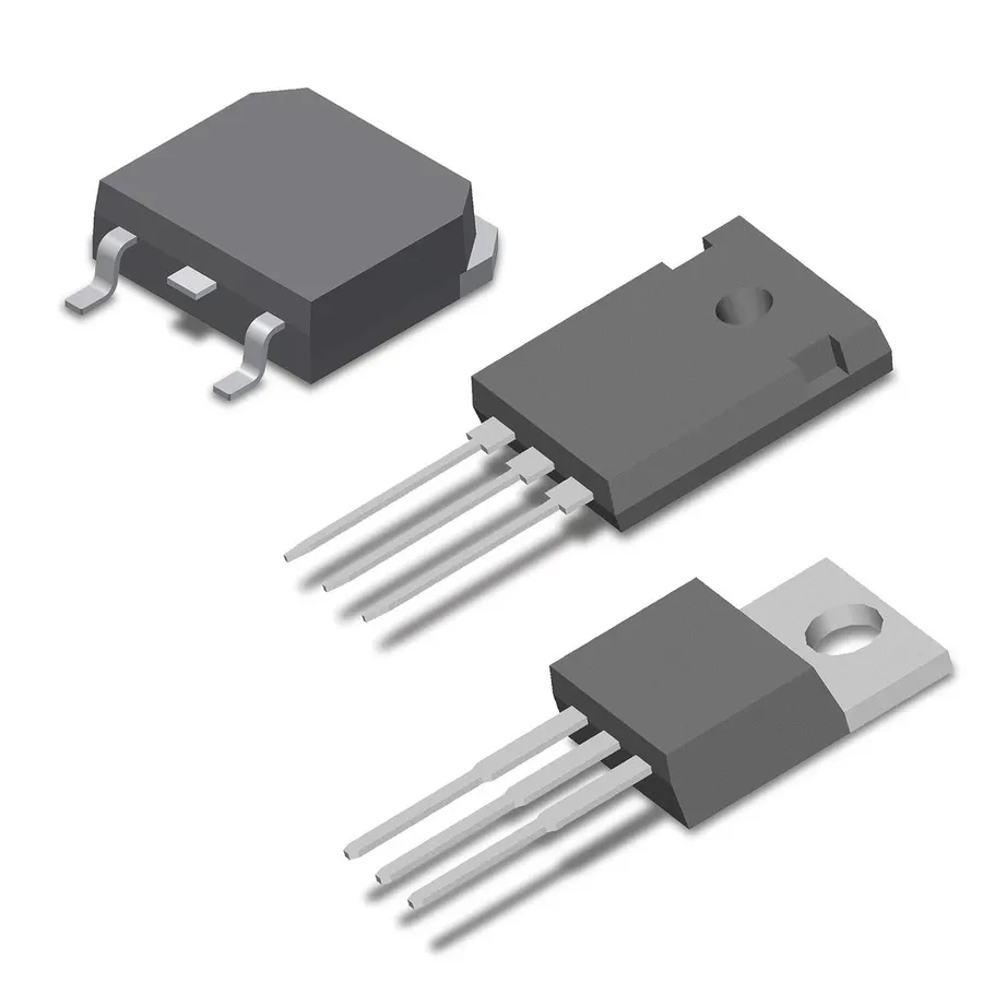
Metal-Oxide-Semiconductor Field-Effect Transistors (MOSFETs), a dominant force in modern electronics, come in two primary flavors: enhancement-mode and depletion-mode. These modes dictate how the gate voltage influences the channel's conductivity, leading to different operational characteristics and application suitability. Understanding these distinctions is crucial for effective circuit design.
| Feature | Enhancement-Mode MOSFET | Depletion-Mode MOSFET |
|---|---|---|
| Channel at Vgs=0 | Non-conducting | Conducting |
| Gate Voltage to conduct | Requires positive Vgs (N-Channel), negative Vgs(P-Channel) | Requires negative Vgs (N-Channel), positive Vgs(P-Channel) to reduce conduction. |
| Typical application | Switching and amplification | Load device, analog switches |
| Symbol | Discontinuous Channel line | Solid Channel line |
| Conduction behavior | Normally OFF (No current flow at Vgs=0) | Normally ON (Current flow at Vgs=0) |
Enhancement-mode MOSFETs are the more commonly used type, acting like a normally-off switch. When no voltage is applied to the gate (Vgs=0), there is no channel to conduct current between the source and drain. The channel is created or enhanced by applying a voltage to the gate terminal. Depletion-mode MOSFETs, on the other hand, operate as normally-on devices. They have a built-in channel that allows current flow even when no voltage is applied to the gate. To turn them off or reduce current flow, a gate voltage must be applied to deplete the channel of charge carriers. Both types are pivotal, with the selection based on circuit requirements.
The selection between enhancement and depletion mode MOSFETs is primarily application-driven. Enhancement MOSFETS are ideal for switching applications and power electronics where they need to be turned on and off, for instance, a high-side switch where the load is connected to the positive supply. Depletion MOSFETs, by contrast, are most often found in analog circuits to make current sources, where they function as the active load, or in applications that require a normally-on switch, like a fail-safe system.
Understanding the key electrical characteristics of Field-Effect Transistors (FETs) is crucial for effective circuit design and application. These characteristics dictate how a FET will behave within a circuit and include parameters like input impedance, transconductance, and switching speed. Each of these parameters influences the performance of the circuit and is a critical element to consider during the design process.
| Characteristic | Description | Impact on Circuit Performance |
|---|---|---|
| Input Impedance | The resistance seen by the input signal source. FETs have very high input impedance. | Minimizes loading on the signal source, allowing for efficient signal transfer with minimal signal loss. This is especially beneficial in amplifier circuits and high-frequency applications. |
| Transconductance (gm) | The ratio of change in drain current to the change in gate-source voltage. Expressed in Siemens (S). | Determines the gain of the amplifier. A higher transconductance value leads to greater amplification. It is a crucial factor in determining the signal amplification and output strength of the circuit. |
| Switching Speed | The speed at which a FET can transition between the on and off states, dependent on the intrinsic capacitances. | Determines how quickly the FET can respond to changes in gate voltage. Faster switching speeds are necessary for high-frequency and high-speed digital applications, while low switching speeds are adequate for less demanding applications. It is particularly crucial in pulse width modulation (PWM) circuits and fast-switching power applications |
| Drain Resistance (rd) | The resistance between the drain and source terminals when the FET is in its active region. | Affects the output impedance of the circuit and influences the overall gain and efficiency. Lower drain resistance results in a lower output impedance. This allows the circuit to deliver more power to the load efficiently |
| Output Impedance | The resistance seen at the output terminal. | Affects how well the circuit can drive a load. A low output impedance is desirable for effective power transfer. |
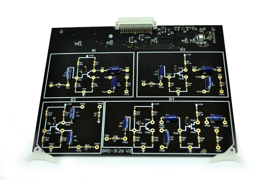
Field-Effect Transistors (FETs) are foundational components in modern electronics, enabling a wide array of applications across diverse industries. Their ability to control current with an electric field, coupled with their high input impedance, makes them ideal for both amplification and switching functions. This section explores the specific uses of FETs in key sectors, highlighting their versatility and impact.
| Application | Industry Example | FET Type | Key Function |
|---|---|---|---|
| Audio Amplification | Home Stereo Systems, Musical Instruments | JFET, MOSFET | Signal amplification with high impedance |
| Switching Power Supplies | Laptop Adapters, Server Power Systems | MOSFET | Efficient power conversion |
| Microprocessors | Computers, Smartphones, Embedded Systems | MOSFET | Logic switching, high speed operation |
| Battery Chargers | Electric Vehicles, Power Tools | Power MOSFET | Switching current to charge batteries |
| Sensor Interfaces | Medical Equipment, Industrial Controls | ISFET, JFET | Detection and transduction of environmental conditions |
Field-Effect Transistors (FETs) offer significant advantages in electronic circuit design, notably their high input impedance and low power consumption, which stem from their unique mode of operation. However, these advantages are balanced by certain limitations, particularly their susceptibility to electrostatic discharge (ESD) and, in some cases, lower transconductance compared to bipolar junction transistors (BJTs).
| Characteristic | FET Transistors | Bipolar Junction Transistors (BJTs) |
|---|---|---|
| Input Impedance | High (Megohms) | Low (kOhms) |
| Power Consumption | Low | Moderate to High |
| Current Control | Voltage Controlled | Current Controlled |
| Transconductance | Moderate to High (depending on type) | High |
| Susceptibility to ESD | High | Low |
| Switching Speed | Fast | Fast |
| Temperature Stability | Good | Moderate |
The high input impedance of FETs minimizes loading effects on preceding stages in a circuit, which means they require very little current to drive. This characteristic is crucial in applications where signal integrity is vital, such as high-frequency amplifiers. In contrast, the current-controlled nature of BJTs results in lower input impedances and higher power consumption, especially at higher frequencies. The transconductance in FETs, while often lower than BJTs, is typically sufficient for most applications and offers very high gain in certain modes. While FETs have many advantages, electrostatic discharge poses a problem, which is why they require careful handling. BJTs tend to be more robust in this area.
This section addresses common queries regarding Field-Effect Transistors (FETs), providing clarity on their distinctions, advantages, and applications. Understanding these frequently asked questions is crucial for both newcomers and seasoned professionals in electronics.
The field of FET transistor technology is in constant evolution, driven by the demand for faster, smaller, and more energy-efficient electronic devices. Current research and development efforts are focused on novel materials, advanced fabrication techniques, and innovative device architectures to overcome the limitations of traditional silicon-based FETs.
Here we delve into some of the most promising trends shaping the future of FET technology:
The relentless pursuit of miniaturization, coupled with the exploration of novel materials and device architectures, ensures that FET transistor technology will remain at the forefront of technological innovation. These trends are expected to shape the next generation of electronics, enabling more powerful, energy-efficient, and versatile devices for a wide range of applications.
FET transistors are indispensable components that have revolutionized the field of electronics. Their ability to control current flow through an electric field makes them incredibly versatile and efficient. From the simplest circuits to the most advanced technologies, the FET transistor remains at the heart of modern electronics, paving the way for innovation. Understanding their principles and applications is essential for anyone looking to grasp the nuances of electronic engineering. As technology evolves, the FET transistor will continue to be a critical element in the future of electronic devices, demonstrating the lasting impact of this invention.

