In the realm of modern electronics, where precision and adaptability are paramount, the varicap diode emerges as a versatile component. Imagine a device that can change its capacitance simply by varying an applied voltage - this is the essence of the varicap, or varactor, diode. From tuning your car radio to enabling sophisticated communication systems, this seemingly simple semiconductor device plays a crucial role, manipulating capacitance like a finely tuned dial. This article will demystify the varicap diode, exploring its inner workings, diverse applications, and why it's a staple in modern circuit design. We will also dive into its characteristics and how it compares to other types of diodes.
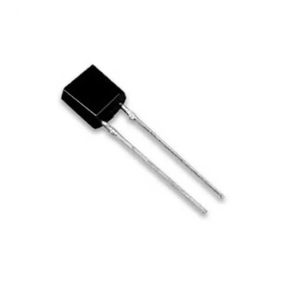
Varicap diodes, also known as varactor diodes, are semiconductor devices engineered to exhibit a variable capacitance that is controlled by the reverse bias voltage applied across their terminals. At its core, a varicap diode leverages the properties of a PN junction to achieve this variable capacitance.
The fundamental structure of a varicap diode is based on a PN junction, which is a boundary between two types of semiconductor materials: P-type (with an excess of holes) and N-type (with an excess of electrons). At the junction, these charge carriers diffuse across the boundary, creating an area devoid of free charge carriers known as the depletion region, or depletion layer. The width of this depletion region is critical, as it determines the capacitance of the diode. Under reverse bias conditions, the depletion region widens, acting as the dielectric of a capacitor, the P and N regions act as the plates, and the depletion region's width becomes the distance between the capacitor plates.
Applying a reverse bias voltage (negative voltage to the P-side and positive voltage to the N-side) to a varicap diode increases the width of the depletion region and reduces the capacitance of the diode, and reducing the reverse bias voltage decreases the depletion region width, and increases capacitance. The change in the depletion region width is directly proportional to the applied reverse bias voltage, thus allowing precise control of the diode's capacitance. This effect is what makes varicap diodes so valuable in tuning circuits.
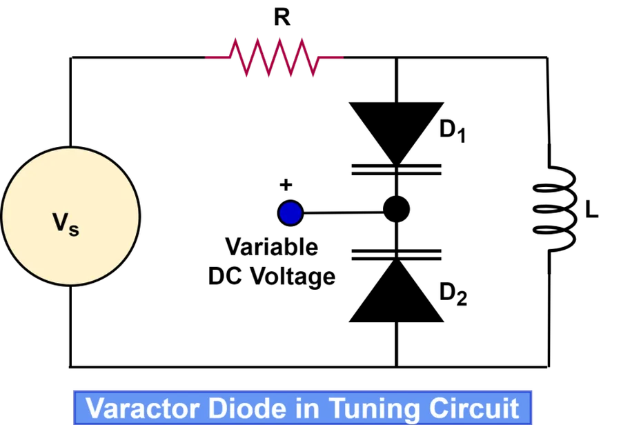
The operational principle of a varicap diode hinges on the modulation of its internal capacitance by an applied reverse bias voltage. This unique characteristic arises from the behavior of the depletion region at the PN junction, which acts as the dielectric of a capacitor, and whose width is directly influenced by the reverse bias voltage.
The key to understanding a varicap diode lies in the manipulation of its depletion region. This region, devoid of mobile charge carriers, forms at the junction between the P-type and N-type semiconductor materials. When a reverse bias is applied, it effectively widens the depletion region. Conversely, decreasing the reverse bias narrows this region. Since capacitance is inversely proportional to the distance between capacitor plates (in this case, the depletion region width), altering this width leads to a direct modulation of the diode's capacitance.
The relationship between the applied reverse voltage and the capacitance is not linear, but rather follows a power-law relationship described by the formula C ∝ V^(-n), where C is the capacitance, V is the reverse voltage, and 'n' is a constant that depends on the doping profile of the diode. This non-linear relationship is critical to its functionality, allowing for a controlled change in capacitance over a specific voltage range. Typically 'n' ranges from 0.3 to 0.5.
| Parameter | Description | Effect on Capacitance |
|---|---|---|
| Reverse Voltage Increase | Increased reverse bias voltage applied to the diode. | Depletion region widens; capacitance decreases. |
| Reverse Voltage Decrease | Decreased reverse bias voltage applied to the diode. | Depletion region narrows; capacitance increases. |
| Depletion Region Width | The width of the depletion region at the PN junction. | Inversely proportional to the capacitance. |
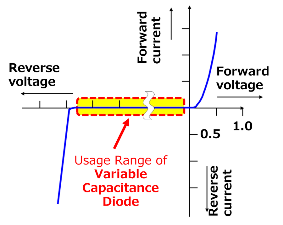
Varicap diodes, also known as varactor diodes, are characterized by their voltage-dependent capacitance, a feature that makes them indispensable in various tuning and frequency control applications. Understanding their key electrical parameters is crucial for effective circuit design and component selection. These parameters include capacitance range, tuning ratio, and quality factor (Q).
| Characteristic | Description | Importance in Application |
|---|---|---|
| Capacitance Range | The range of capacitance values achievable by varying the reverse bias voltage. | Determines the tuning range of the circuit. A wider range allows for a greater adjustment of frequency. |
| Tuning Ratio | The ratio between the maximum and minimum capacitance of the diode, typically expressed as Cmax/Cmin. | A higher tuning ratio enables a wider range of frequency adjustment. |
| Quality Factor (Q) | A measure of the diode's energy loss, indicating its efficiency as a capacitor. Higher Q values imply lower losses. | Critical for low-noise and high-performance circuits. Lower Q results in higher losses and reduced performance. |
| Reverse Leakage Current | The current that flows through the diode when it is reverse biased. | Should be minimized as it can affect the stability of the circuit, particularly at high frequencies. High leakage current indicates a lossy diode. |
| Temperature Coefficient | How capacitance changes with temperature. | Important in environments with temperature variation. Affects the stability and predictable performance of the circuit. |
| Breakdown Voltage | The reverse voltage at which the diode starts to conduct significantly. | Must be higher than the maximum reverse bias voltage applied in the circuit to prevent diode damage. |
When selecting a varicap diode for a specific application, carefully consider these characteristics based on the specific circuit requirements. The trade-offs between capacitance range, tuning ratio, Q factor, and temperature stability will significantly affect the performance and reliability of the design.
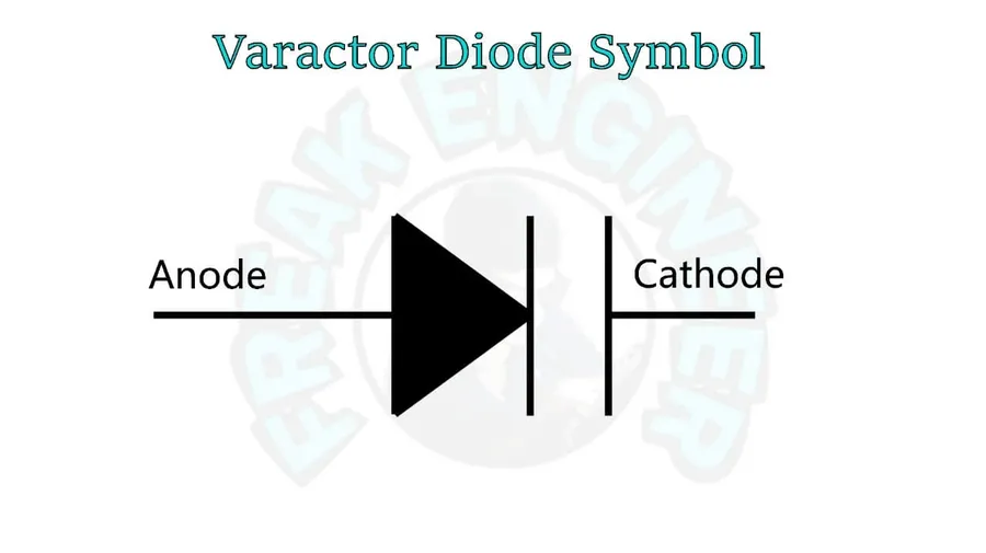
Understanding the schematic symbols for varicap diodes is crucial for accurately interpreting and designing electronic circuits. These symbols, while often similar to standard diode symbols, incorporate unique features to indicate their variable capacitance behavior. This section delineates the commonly used symbols and their representation in circuit diagrams.
It is essential to note that while the symbols may vary in their specifics, they all convey the same fundamental property: the varicap diode's capacitance is dependent on the applied voltage. When interpreting circuit schematics, always check the legend or component list to confirm the symbol's meaning and ensure clarity in design interpretations.
Varicap diodes, with their voltage-dependent capacitance, are indispensable in numerous electronic applications, particularly those requiring precise and adjustable tuning. Their ability to function as voltage-controlled capacitors makes them essential in RF and signal processing circuits.
The terms 'varicap' and 'varactor' are often used interchangeably within the electronics field, referring to a semiconductor diode whose capacitance varies with the reverse voltage applied across its terminals. In essence, they describe the same device, which functions as a voltage-controlled variable capacitor.
While some older literature might attempt to differentiate them, modern usage generally considers them synonymous. There is no practical distinction in terms of physical structure, operational principle, or typical applications; both terms refer to diodes designed to exploit the variable capacitance of their PN junction's depletion region under varying reverse bias conditions. Therefore, whether one calls it a varicap or a varactor, they are talking about the same component.
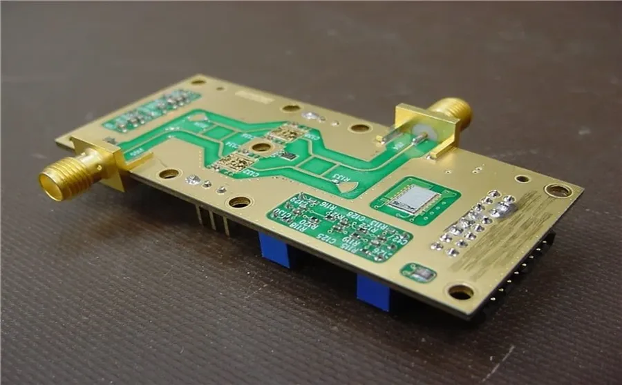
Varicap diodes are indispensable components in modern Radio Frequency (RF) design, providing precise and electrically controllable capacitance crucial for advanced communication systems. Their ability to vary capacitance with applied voltage enables sophisticated tuning, impedance matching, and frequency control, making them essential for high-performance RF circuits.
The integration of varicap diodes into advanced circuit designs has been facilitated by the development of highly linear and low-loss diodes. These modern devices offer lower series resistance and higher Q values, enabling more precise control over RF signals and lower signal losses and improved power efficiency in modern designs. Additionally, improvements in manufacturing processes have made varicap diodes more compact and reliable, which is highly important for high-density, miniaturized devices.
This section addresses common questions regarding varicap diodes, providing clarity on their limitations, selection criteria, and how they compare to other diode types. These frequently asked questions (FAQs) are designed to offer practical insights for engineers and enthusiasts working with these versatile components.
Successfully integrating varicap diodes into circuit designs requires careful consideration of several practical factors. These include impedance matching to maximize power transfer, the precise selection of bias voltage to achieve the desired capacitance, and accounting for thermal effects which can alter performance.
In conclusion, the varicap diode is a testament to the ingenuity of semiconductor technology, providing a means of electronically controlling capacitance. From tuning radios to enabling intricate communication systems, the varicap's versatility and precision make it an indispensable component in modern electronic design. Understanding its principles, characteristics, and diverse applications not only showcases the intricacies of semiconductor physics but also empowers engineers and enthusiasts alike to implement sophisticated solutions. The varicap diode's ability to vary capacitance via voltage is not merely a technical curiosity; it is the foundation upon which much of our modern communication and electronic landscape is built, a tiny component with a very large impact.

