In today's fast-paced world of multimedia and broadcasting, the demand for seamless and high-quality video switching is paramount. At the heart of every video switcher lies a sophisticated Printed Circuit Board (PCB) that orchestrates the complex routing and processing of video signals. Zero One Solution Limited, a leader in rapid PCB prototyping and manufacturing, offers comprehensive Video Switcher PCB solutions designed to meet the rigorous demands of modern video technology. With the increasing complexity of video formats and the need for real-time performance, a well-designed PCB is crucial. This article delves into the intricacies of Video Switcher PCB solutions, highlighting the design considerations, manufacturing processes, and assembly expertise required to create robust and reliable video switching systems. Explore how Zero One Solution empowers innovation in video technology through cutting-edge PCB solutions.
Understanding Video Switcher PCBs
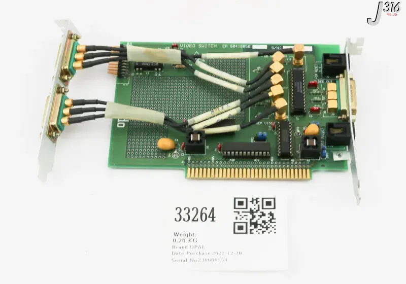
Video Switcher PCB
Video switcher PCBs are the foundational electronic assemblies that enable the seamless routing, processing, and distribution of video signals in a myriad of applications, from broadcast studios and live events to medical imaging and surveillance systems. Their critical role lies in their ability to manage multiple video inputs and outputs, ensuring signal integrity, minimizing latency, and maintaining high-fidelity visual data. A meticulously engineered PCB is paramount for optimal performance, as any degradation in signal quality at this core level can significantly impact the final video output, affecting everything from color accuracy to resolution and frame rate.
What are Video Switcher PCBs? Video Switcher PCBs (Printed Circuit Boards) are specialized circuit boards designed to handle the complex routing and processing of various video input signals to one or more output destinations. They integrate components like high-speed differential signal traces, video processors, multiplexers, and demultiplexers to manage diverse video standards such as HDMI, SDI, DisplayPort, or analog composite/component signals. Their primary function is to provide a robust and efficient platform for selecting, combining, or distributing video streams without introducing signal degradation or latency, which is crucial for real-time video applications.
The operational efficiency of a video switcher is directly proportional to the quality of its underlying PCB. In essence, these PCBs act as the central nervous system of video systems, dictating how effectively video streams are managed and presented. Therefore, understanding their intricate design and functional requirements is the first step towards developing high-performance video solutions.
Key Design Considerations for Video Switcher PCBs
Designing a robust Video Switcher PCB demands meticulous attention to several critical factors that directly influence signal quality and overall system reliability. Achieving high-performance video switching necessitates precision engineering in areas such as signal integrity, controlled impedance, and effective thermal management. These foundational design considerations are paramount to delivering the pristine video output required for professional broadcasting, live events, and advanced multimedia applications.
Signal Integrity (SI) Signal integrity is the bedrock of high-performance video switcher PCBs. It refers to the quality of electrical signals as they travel through the circuit, minimizing distortion, noise, and data loss. For video signals, this translates directly to picture clarity and fidelity. Maintaining signal integrity involves careful trace routing, minimizing crosstalk between adjacent traces, and avoiding sharp bends that can cause reflections. Advanced simulation tools are often employed to predict and mitigate SI issues early in the design phase.
Impedance Control Consistent impedance is crucial for high-speed digital and analog video signals. Mismatched impedance can lead to signal reflections, causing ghosting, blurring, and reduced video quality. Designers must carefully calculate and maintain the characteristic impedance of traces to match the source and load impedances, typically 50 or 75 ohms for video applications. This involves precise control over trace width, dielectric constant of the PCB material, and the distance to the reference plane (ground or power).
Thermal Management High-performance video processing components, such as FPGAs, ASICs, and high-speed serializers/deserializers (SerDes), generate significant heat. Effective thermal management is vital to prevent component overheating, which can lead to performance degradation, instability, or even premature failure. Strategies include incorporating thermal vias, using heat sinks, optimizing copper pour for heat dissipation, and selecting PCB materials with good thermal conductivity. Proper airflow design within the enclosure is also a critical consideration.
Power Delivery Network (PDN) A stable and clean power supply is essential for sensitive video circuitry. A well-designed Power Delivery Network (PDN) minimizes voltage fluctuations and noise, ensuring reliable operation of integrated circuits. This involves strategic placement of decoupling capacitors, proper plane design for power and ground, and careful consideration of current paths to reduce inductive effects and voltage drops. Poor PDN design can introduce noise that manifests as artifacts in the video output.
Layer Stack-up Optimization The PCB layer stack-up significantly impacts signal integrity and EMI performance. For video switchers, a multi-layer board is typically required to provide dedicated signal layers, power planes, and ground planes. Optimizing the stack-up involves selecting the appropriate number of layers, determining the thickness of dielectric materials, and strategically placing signal layers adjacent to ground or power planes to create controlled impedance environments and provide shielding against electromagnetic interference (EMI).
Material Selection for High-Performance Video Switching
Selecting optimal PCB materials for video switchers is paramount for achieving high-fidelity signal transmission and overall system reliability. The inherent demands of video signals, particularly high-bandwidth uncompressed streams, necessitate substrates with stable dielectric properties, minimal signal loss, and efficient thermal dissipation. Substandard material choices can lead to signal degradation, impedance mismatches, and premature component failure, directly impacting the video switcher's performance and longevity. Therefore, a meticulous material selection process is not merely a design consideration but a foundational pillar for professional-grade video switching solutions.
Why is material selection critical for video switcher PCBs? Material selection for video switcher PCBs is critical because it directly impacts signal integrity, impedance control, and thermal management. High-frequency video signals are highly susceptible to signal loss and distortion if the PCB material has an unstable dielectric constant or high dissipation factor. Furthermore, effective heat dissipation is essential for the long-term reliability and performance of active components on the board. The right materials ensure consistent signal propagation, minimize crosstalk, and prevent overheating, all of which are vital for maintaining high-quality video output across various resolutions and frame rates.
Material Type
Key Properties
Typical Applications for Video Switchers
FR-4
Good balance of electrical, mechanical, and thermal properties; cost-effective
Lower-frequency or less demanding video switching applications, control circuitry
High-Tg FR-4
Higher glass transition temperature; improved thermal stability under stress
High-power video switchers or applications with significant heat generation
Low-Loss Laminates (e.g., Rogers, Isola)
Low dielectric loss (Df), stable dielectric constant (Dk) over frequency, excellent signal integrity
High-definition (HD), 4K, 8K video switchers, broadcast and professional AV equipment
Ceramic/Hybrid Materials
Exceptional thermal conductivity, very low Dk and Df, high-frequency stability
Specialized ultra-high-frequency video applications, power amplifiers within video switchers
The choice of PCB material is a nuanced decision, balancing performance requirements with cost and manufacturability. For cutting-edge video switchers handling uncompressed 8K or even 12K signals, the focus shifts heavily towards advanced low-loss laminates. These materials, such as those from Rogers Corporation or Isola Group, are engineered to minimize signal attenuation at high frequencies, preserving the fidelity of the video stream. Their stable dielectric constant ensures consistent impedance, critical for preventing reflections and maintaining signal integrity. For projects with less stringent bandwidth demands or where cost is a primary constraint, enhanced FR-4 or High-Tg FR-4 variants can still offer a robust and reliable foundation. Ultimately, a deep understanding of the video signal's characteristics and the operational environment is crucial for making the most informed material selection, ensuring the final product meets the rigorous demands of professional video applications.
Manufacturing Processes for Video Switcher PCBs
PCB Etching
The production of high-performance video switcher PCBs demands meticulous manufacturing processes that ensure signal integrity and robust reliability. Each stage, from initial design translation to final surface treatment, requires precise execution and stringent quality control. This commitment to detail is paramount, as any deviation can compromise the critical high-speed signal routing inherent in video switching applications.
Data Preparation and Imaging The manufacturing process begins with converting the PCB design into manufacturing data, including Gerber files. This data is then used to create phototools, which are photographic films containing the circuit patterns. These phototools are used to expose photosensitive resist material laminated onto the copper-clad laminate, precisely transferring the circuit image onto the substrate.
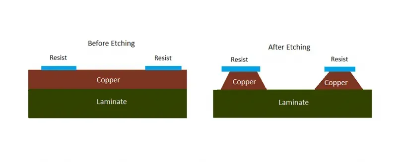
Etching: Defining the Circuitry Following imaging, the exposed photosensitive resist hardens, protecting the underlying copper. The board then undergoes an etching process, typically using chemical solutions, to remove the unwanted copper from the unexposed areas. This selectively removes copper, leaving behind the precisely defined circuit traces, pads, and other features essential for video signal transmission.
Layer Lamination and Pressing For multi-layer video switcher PCBs, individual core layers, each with etched circuitry, are carefully aligned and bonded together under high temperature and pressure using prepreg (pre-impregnated) materials. This lamination process creates a single, integrated multi-layer board, ensuring mechanical stability and precise electrical connections between layers critical for complex video signal routing.
Drilling and Plating Once laminated, holes are drilled through the PCB for component leads and vias (vertical interconnect access) that connect different layers. These drilled holes are then metallized through an electroless and electrolytic plating process, creating a conductive path for electrical signals between layers. This ensures robust and reliable interconnections across the PCB's vertical dimension.
Solder Mask Application and Legend Printing A protective solder mask layer is applied over the copper traces, except for the pads where components will be soldered. This layer prevents solder bridges during assembly and protects the circuitry from environmental factors. Finally, a silkscreen legend is printed, adding component designators, polarity indicators, and other helpful markings for assembly and troubleshooting.
Surface Finishing The exposed copper pads are then coated with a surface finish, such as ENIG (Electroless Nickel Immersion Gold), HASL (Hot Air Solder Leveling), or OSP (Organic Solderability Preservative). This finish protects the copper from oxidation, ensures excellent solderability during component assembly, and provides a reliable interface for electrical connections, crucial for the longevity and performance of video switcher PCBs.
Assembly and Testing of Video Switcher PCBs
PCB Soldering
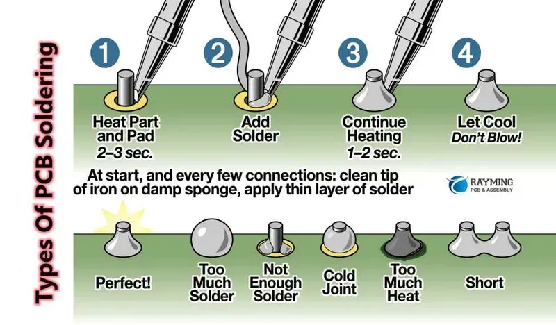
The successful deployment of a high-performance video switcher PCB hinges critically on meticulous assembly and rigorous testing protocols. These stages are not merely procedural but integral to validating the integrity of the design and the quality of manufacturing, ultimately ensuring the PCB's reliability and optimal functionality in demanding video environments. Precision in component placement, adherence to advanced soldering techniques, and comprehensive post-assembly inspections are paramount to achieving the pristine signal integrity required for seamless video switching operations.
Component Placement and Mounting for Video Switcher PCBs Accurate component placement on video switcher PCBs is crucial for maintaining signal integrity, especially for high-frequency video signals. Automated Pick-and-Place machines ensure precise positioning of surface-mount devices (SMDs) and through-hole components, minimizing parasitic effects and signal degradation. Component orientation, spacing, and thermal considerations are meticulously controlled to prevent crosstalk and ensure proper heat dissipation, vital for sustained performance in video applications with high data rates and processing loads. Verification through Automated Optical Inspection (AOI) after placement identifies any misalignments or missing components before soldering, ensuring foundational quality before thermal processing begins, thereby reducing rework and improving overall yield for complex video switcher designs.
Soldering Technique
Description
Application for Video Switcher PCBs
Advantages
Disadvantages
Reflow Soldering
Components are placed on solder paste, then heated in a reflow oven to melt the solder and form connections.
Ideal for high-density SMDs prevalent in video switcher PCBs, ensuring uniform and strong connections.
High throughput, excellent for fine-pitch components, repeatable process.
High initial equipment cost, sensitive to temperature profiles.
Wave Soldering
PCBs pass over a molten wave of solder, primarily for through-hole components.
Used for components that cannot withstand reflow temperatures, or for mixed-technology boards.
Cost-effective for large batches of through-hole components, strong mechanical bonds.
Not suitable for fine-pitch SMDs, potential for solder bridging or skips.
Selective Soldering
A precise, localized wave of solder targets specific through-hole components.
Optimal for mixed-technology PCBs with both SMD and a few through-hole components, minimizing thermal stress.
Precise application, ideal for heat-sensitive components, reduces bridging.
Lower throughput than wave soldering, higher complexity for programming.
Quality Inspection and Testing Methodologies for Video Switcher PCBs Robust quality inspection and testing are indispensable for video switcher PCBs to guarantee flawless operation. In-Circuit Testing (ICT) verifies component presence, correct values, and short/open circuits, while Functional Testing (FCT) simulates real-world video signal paths to confirm the PCB meets design specifications, including video signal quality, switching speed, and latency. Environmental Stress Screening (ESS) or Burn-In Testing subjects the PCBs to extreme temperatures and humidity to detect latent defects before deployment. High-speed signal integrity testing, utilizing oscilloscopes and vector network analyzers, is critical to ensure minimal signal loss and distortion, paramount for high-resolution video streams. These comprehensive testing regimes, including Electromagnetic Compatibility (EMC) testing, validate the PCB's performance under various operating conditions, ensuring the video switcher delivers consistently high-quality output without interference, and adhering to broadcast and AV industry standards like SMPTE and HDMI.
The Role of Rapid Prototyping in Video Switcher Development
Rapid prototyping is a transformative force in the development of Video Switcher PCBs, enabling engineers to swiftly validate designs, identify potential issues early, and accelerate the journey from concept to market-ready product. This agile approach is critical in the fast-evolving video technology landscape, where rapid iteration and performance optimization are paramount for maintaining a competitive edge and ensuring seamless functionality in complex video signal routing applications.
How does rapid prototyping accelerate Video Switcher PCB development? Rapid prototyping accelerates Video Switcher PCB development by allowing for the quick creation of physical prototypes from digital designs. This enables engineers to perform early-stage testing and validation of signal integrity, impedance control, and thermal performance, significantly reducing design cycles and preventing costly errors later in the development process. It fosters an iterative design approach, where design modifications can be implemented and re-tested almost immediately, streamlining the entire development timeline and leading to faster time-to-market for advanced video switching solutions.
Zero One Solution's Expertise in Video Switcher PCB Solutions
PCB Prototype
Zero One Solution Limited stands at the forefront of providing comprehensive PCB solutions for the demanding realm of video switchers. Our two decades of experience, coupled with a deep understanding of signal integrity, high-speed data transmission, and compact design, position us as a premier partner for innovating and manufacturing high-performance video switcher PCBs. From the initial conceptualization and precise design, through the intricate manufacturing processes, to meticulous assembly and rigorous testing, we offer a seamless, end-to-end service that ensures your video switching products achieve unparalleled reliability and performance. Our commitment to rapid prototyping significantly accelerates your time-to-market, allowing for agile development and validation of cutting-edge video technologies.
Comprehensive PCB Design & Engineering Leveraging advanced simulation tools and deep expertise, our engineers meticulously design video switcher PCBs, prioritizing signal integrity, impedance control, EMI/EMC compliance, and thermal management to prevent signal degradation and ensure stable operation, even in high-bandwidth applications.
Advanced Manufacturing Capabilities With state-of-the-art facilities in Shenzhen, we excel in producing multi-layer PCBs with tight tolerances and complex stack-ups essential for video switchers. Our processes encompass precise etching, reliable plating, and a variety of surface finishes (e.g., ENIG, OSP) to meet stringent performance requirements and environmental resilience standards. We handle both small-batch R&D prototypes and large-scale production runs with consistent quality.
Precision Assembly & Quality Assurance Our assembly services utilize automated SMT and THT lines, ensuring accurate component placement and robust soldering for high-density video switcher boards. We employ stringent quality control measures, including AOI, X-ray inspection, and functional testing, to verify every board's integrity and performance against specified parameters, guaranteeing defect-free solutions.
Service Area
Zero One Solution's Advantage
Impact on Video Switcher PCB
PCB Design
Expertise in high-speed digital and analog signal integrity, impedance matching, and noise reduction.
Ensures pristine video signal transmission, minimal crosstalk, and robust system stability for critical applications like live broadcasting and professional AV installations, supporting resolutions up to 8K and beyond.
Case Studies: Successful Video Switcher PCB Projects
Video Switcher PCB
Zero One Solution Limited consistently delivers high-performance Video Switcher PCB Solutions, demonstrating our deep expertise and commitment to client success through practical application. Our agile rapid prototyping and stringent quality control processes enable us to tackle complex challenges, providing tailored PCB solutions that meet the demanding specifications of modern video switching technologies. These case studies exemplify our capability to transform intricate design requirements into reliable, high-fidelity hardware, significantly contributing to the rapid development and market deployment of cutting-edge video systems for our global clientele.
High-Definition Broadcast Switcher for Live Events A client required a robust PCB solution for a high-definition video switcher intended for live broadcast events, demanding exceptionally low latency and superior signal integrity. Zero One Solution utilized advanced multi-layer PCB design, incorporating precise impedance matching and optimized trace routing to minimize signal degradation. The successful implementation resulted in a switcher capable of seamless, artifact-free transitions for critical live productions, exceeding the client's expectations for performance and reliability under intense operational conditions.
Compact 4K Video Matrix Switch for Professional AV Faced with the challenge of integrating a 4K video matrix switcher into a highly space-constrained professional AV rack, our engineers designed a compact, high-density PCB that maintained uncompromised signal quality for ultra-high-definition video. This involved meticulous component placement, thermal management strategies for efficient heat dissipation within the small form factor, and the selection of low-loss materials suitable for 4K bandwidth. The solution enabled the client to offer a powerful, yet compact, 4K video distribution system, expanding their market reach in professional AV installations.
Custom Medical Imaging Video Switcher PCB For a medical device manufacturer, Zero One Solution developed a custom video switcher PCB for a diagnostic imaging system, which required not only high resolution and fidelity but also adherence to stringent medical safety and EMI/EMC standards. Our design process incorporated specialized shielding techniques, isolated power planes, and robust component selection to ensure both signal purity and regulatory compliance. The resulting PCB contributed to a medical imaging device that provided clear, reliable visuals crucial for accurate diagnoses, underscoring our capability in highly regulated sectors.
Scalable Video Wall Controller PCB A project for a large-scale video wall application demanded a modular and scalable video switcher PCB solution that could handle numerous simultaneous inputs and outputs with zero visual delay. Zero One Solution engineered a PCB architecture supporting high-speed data transfer and efficient synchronization across multiple display segments. The design prioritized signal integrity over long traces and incorporated redundancy features to ensure continuous operation. This project showcased our ability to deliver highly scalable and dependable PCB solutions for complex visual display systems.
Future Trends in Video Switcher PCB Technology
The landscape of video switcher PCB technology is in constant evolution, driven by the insatiable demand for higher resolution, increased bandwidth, and more intelligent signal processing. As a veteran SEO engineer and marketing expert, I can affirm that staying ahead of these trends is paramount for any PCB solution provider aiming to deliver cutting-edge products. The future will see PCBs for video switchers integrating even more sophisticated capabilities, moving beyond simple signal routing to encompass advanced video analytics, real-time compression, and seamless interoperability across diverse ecosystems.
How will higher bandwidth requirements impact future video switcher PCB designs? The transition to 4K, 8K, and even higher resolutions, coupled with increased frame rates and HDR, necessitates PCBs capable of handling multi-gigabit data rates with exceptional signal integrity. This translates to a greater emphasis on low-loss dielectric materials (e.g., those with lower Dk/Df values), advanced impedance control, shorter trace lengths, and sophisticated routing strategies to mitigate crosstalk and signal degradation. Multi-layer designs with optimized stack-ups will become even more critical to manage signal paths efficiently and minimize electromagnetic interference (EMI).
What role will advanced signal processing play in the evolution of video switcher PCBs? Future video switcher PCBs will increasingly incorporate powerful FPGAs (Field-Programmable Gate Arrays) and ASICs (Application-Specific Integrated Circuits) to enable real-time video scaling, color correction, format conversion, and even AI-driven content analysis directly on the board. This requires PCB designs with robust power delivery networks (PDN) to support these high-power, high-performance components, along with optimized thermal management solutions such as advanced heatsinks, thermal vias, and even liquid cooling for densely packed processing units. High-speed interfaces like PCIe and DDR5 will be integral.
How will video switcher PCBs integrate with new video formats and connectivity standards? The proliferation of new video formats (e.g., NDI, SMPTE ST 2110) and evolving connectivity standards (e.g., HDMI 2.1, DisplayPort 2.0, USB4) will demand highly flexible and adaptable PCB designs. This includes support for a wider array of interface types, backward compatibility, and the ability to seamlessly bridge between different protocols. Modularity in PCB design, allowing for easy upgrading or swapping of interface cards, will become a key differentiator, enabling future-proof solutions for diverse professional AV environments.
What are the emerging material trends for high-frequency video switcher PCBs? Beyond traditional FR-4, emerging material trends for high-frequency video switcher PCBs include advanced laminates like Megtron 6, Rogers Corporation materials (e.g., RO4000 series), and Panasonic Megtron 7. These materials offer superior dielectric constants (Dk) stability across frequencies, lower dissipation factors (Df) to minimize signal loss, and improved thermal performance. Research into novel substrate materials and advanced manufacturing techniques like embedded passive technology will further enhance performance and miniaturization.
How will PCB manufacturing and assembly processes adapt for future video switchers? As component sizes shrink and integration density increases, manufacturing and assembly processes will require even greater precision. Advanced techniques such as fine-pitch BGA (Ball Grid Array) assembly, vacuum reflow soldering to eliminate voids, and precise automated optical inspection (AOI) will be standard. Furthermore, the integration of advanced test methodologies, including high-speed functional testing and compliance testing for new video standards, will be crucial to ensure the reliability and performance of complex video switcher PCBs.
In conclusion, Video Switcher PCBs are the unsung heroes of modern video technology, enabling seamless transitions and high-quality signal processing. Zero One Solution Limited stands at the forefront of providing comprehensive PCB solutions for video switchers, offering expertise in design, manufacturing, and assembly. By partnering with Zero One Solution, you gain access to cutting-edge technology, rapid prototyping, and a commitment to quality that ensures your video switching systems perform flawlessly. Elevate your video technology with Zero One Solution's expert PCB solutions. Contact us today to discuss your project and discover how we can accelerate your product development!