Blog

Common PCB Failure Cases and Root Causes: Electrical, Mechanical, and Material

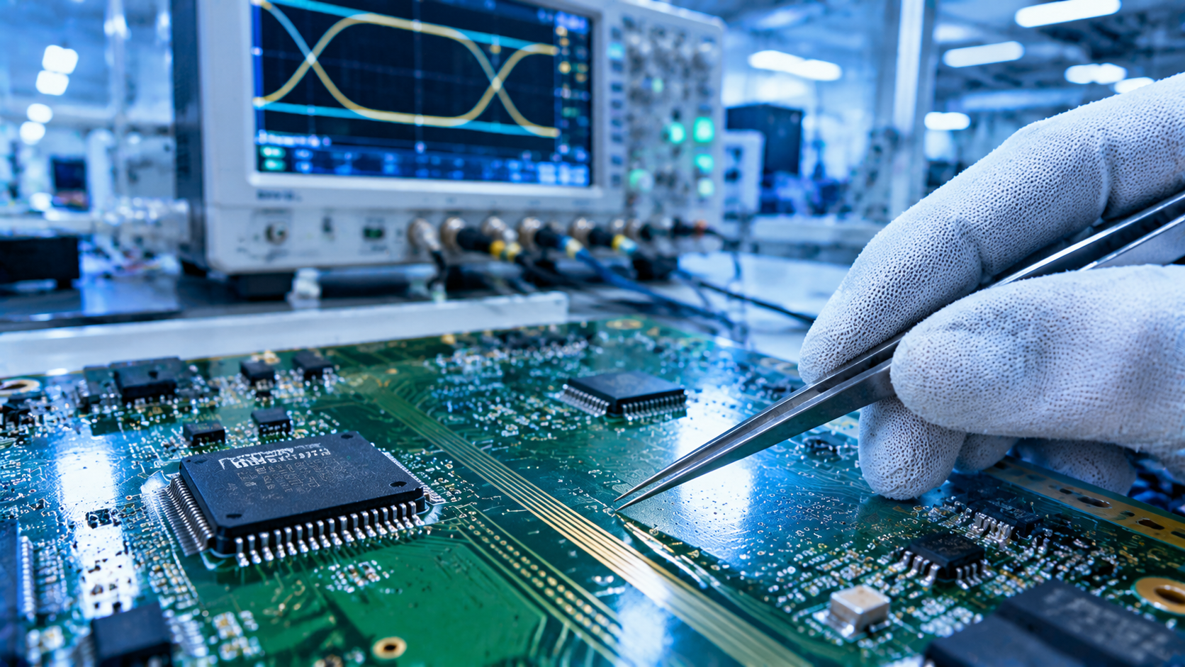
PCB reliability directly affects the stability of electronic devices. This guide covers common PCB failure cases—short circuits, open circuits, signal transmission anomalies, board warpage, component detachment, substrate aging, and solder fatigue—along with their root causes in design, manufacturing, and environmental stress, plus practical prevention measures.

2026.11.02

PCB Design Output Files: A Complete Guide to Manufacturing and Assembly Data

Before a PCB can go into production, you need a complete set of output files—manufacturing data, assembly files, and documentation. This guide covers everything from Gerber and NC drill files to BOM, Pick-and-Place, STEP models, test reports, and special manufacturing notes, helping you package your files correctly for the factory.
2026.11.02

16 Essential PCB Design Principles: From Layout to Routing

A great PCB design isn't just about connectivity—it's about signal integrity, power integrity, and EMC. This guide covers 16 essential PCB design principles organized into three categories: layout strategy, stack-up and plane design, and routing rules. Each principle includes the root cause of the problem and the practical countermeasure.
2026.10.30

The 2026 Hardware Inflection Point: How AI Computing and 800V EVs Are Reshaping PCB Manufacturing

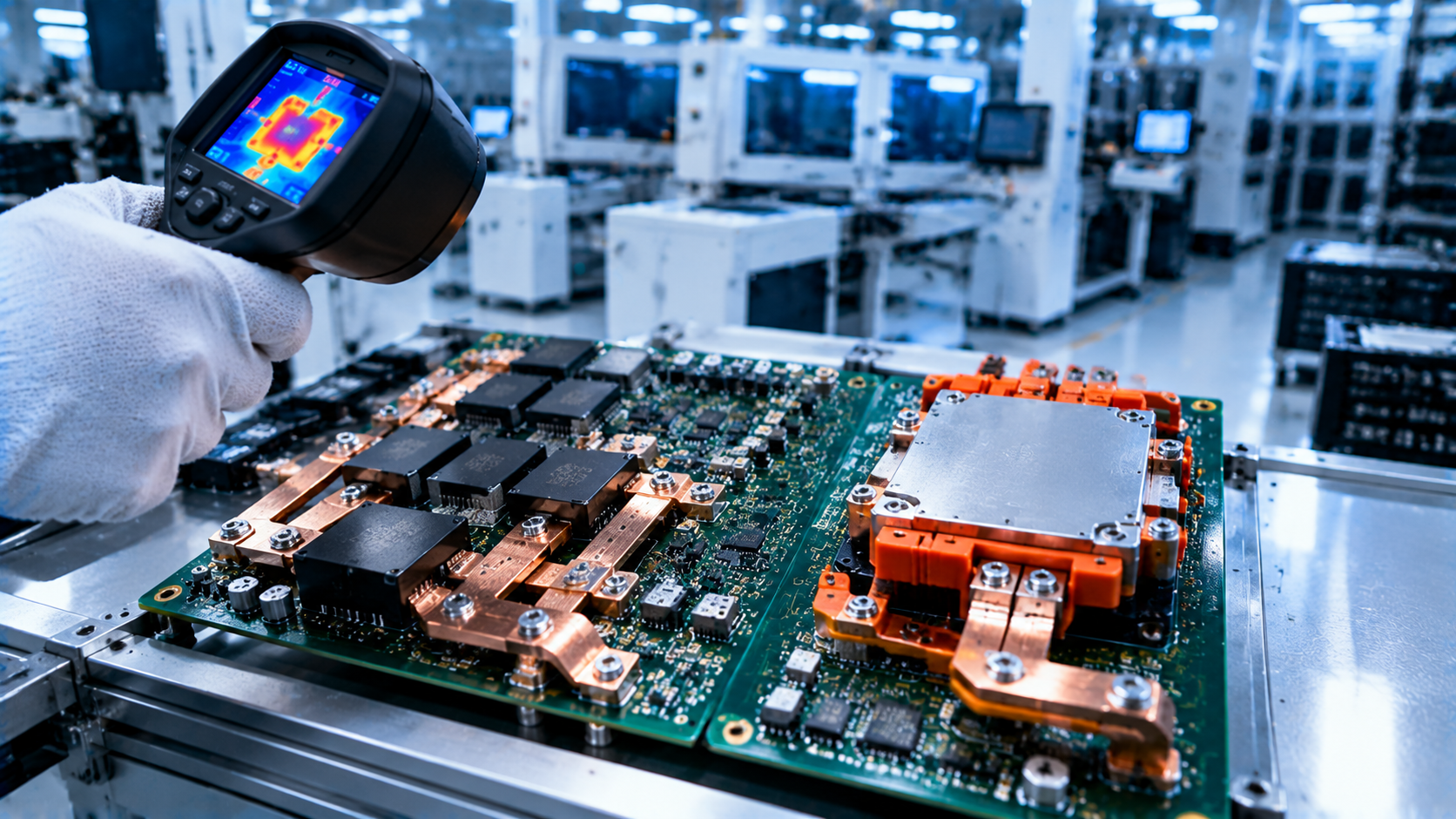
In 2026, the electronics industry is facing extreme physical challenges. AI servers are pushing power consumption past 100kW, and EVs are adopting 800V platforms. This article explores how these trends are driving extreme demands for heavy copper (up to 20oz), high-layer HDI, advanced thermal management, and high-voltage insulation—and how AnyPCBA’s manufacturing capabilities are rising to meet them.
2026.10.30

15 Common PCB Circuit Effects in Electronic Design: Causes and Mitigation

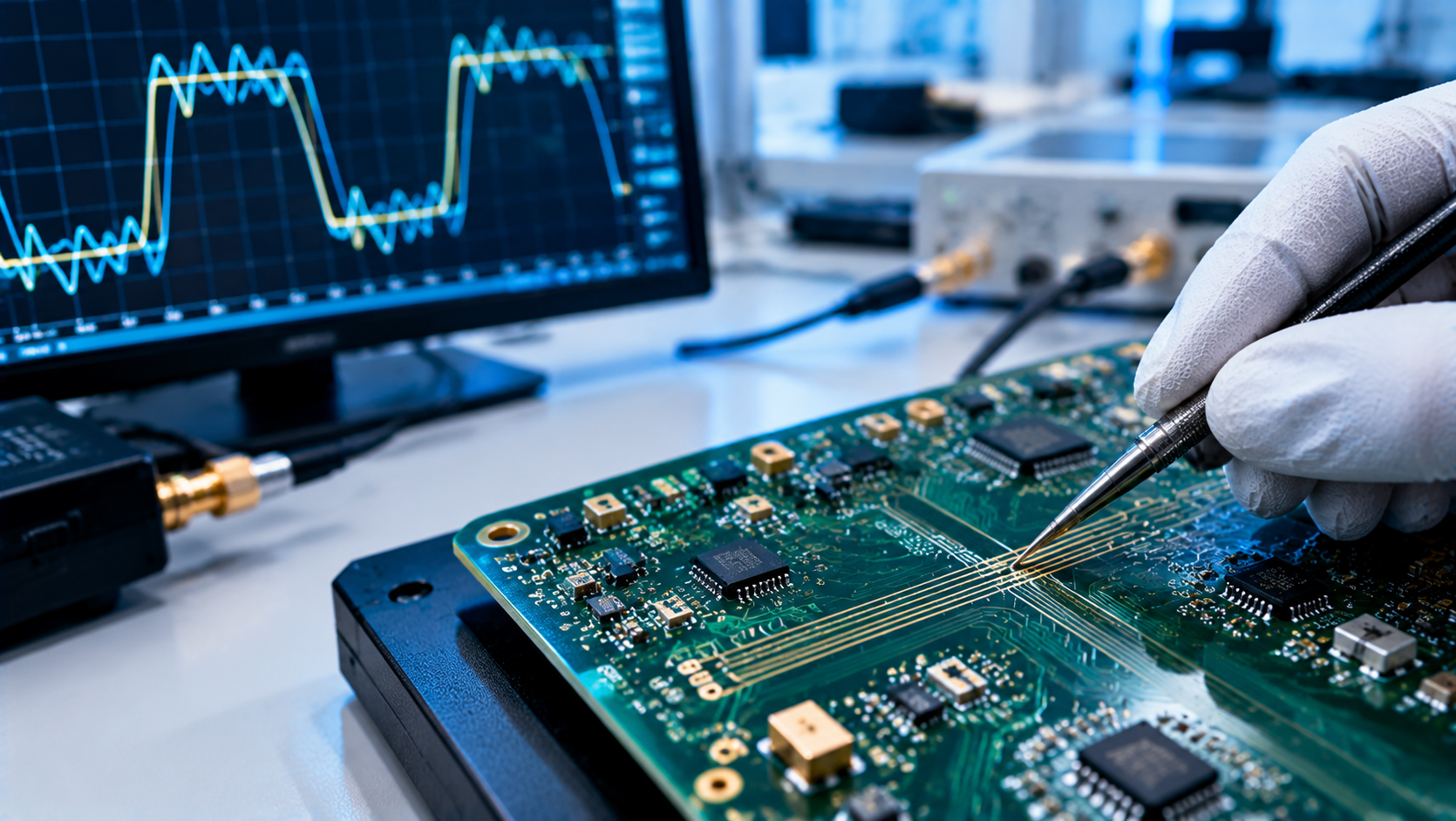
Many PCB failures aren't caused by drawing errors, but by physical effects invisible in schematics and DRC checks. This guide covers 15 common PCB circuit effects—from bridging, ripple, and crosstalk to thermal expansion, via effects, and latent defects—organized into four categories: signal transmission, EMC, environmental physics, and manufacturing reliability.
2026.10.29

Preventing PCB Warpage and Bowing During Reflow Soldering

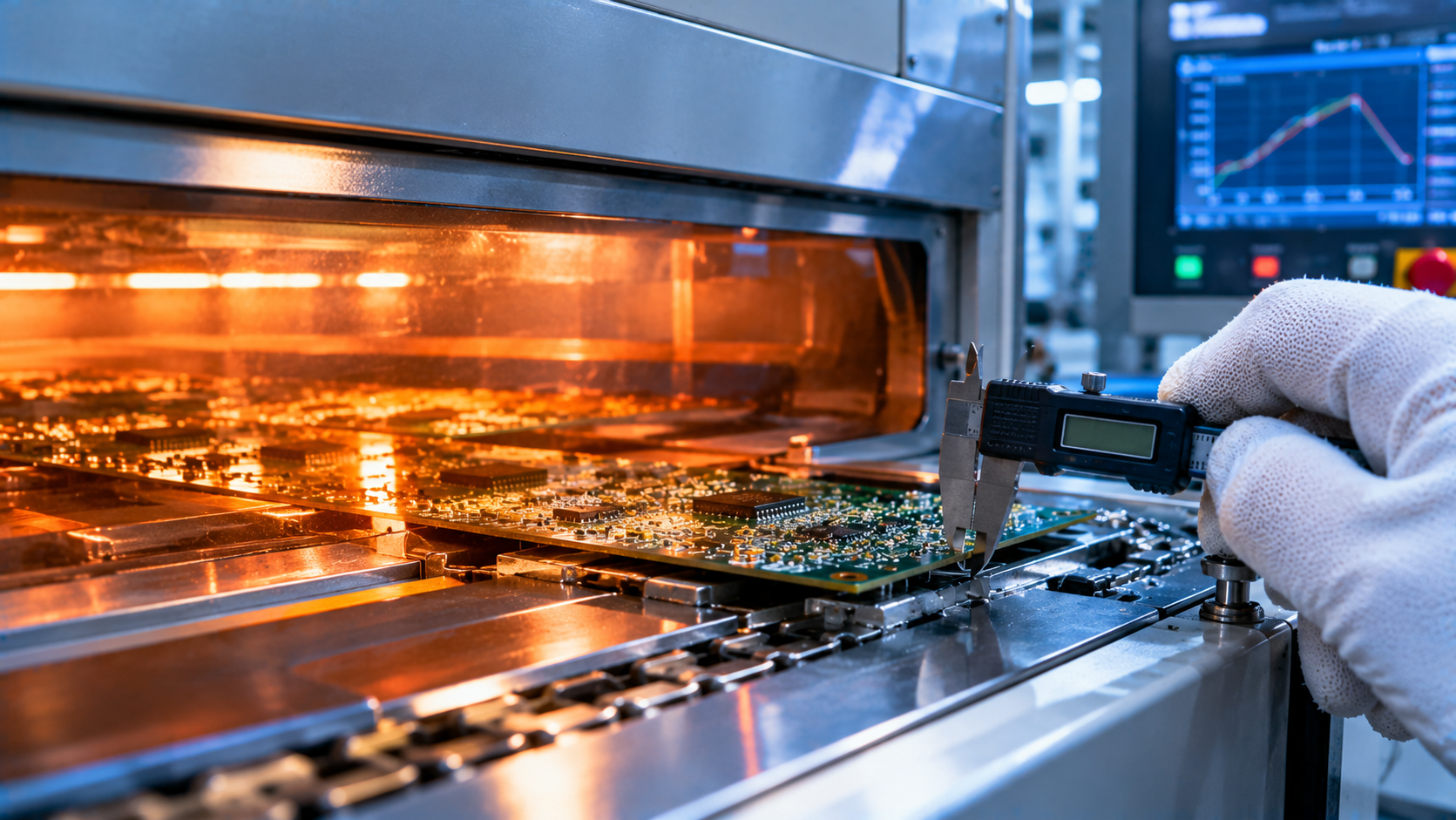
PCB warpage and bowing are common defects during SMT reflow soldering, caused by thermal stress from mismatched CTE between copper, resin, and fiberglass. This article covers five key strategies to prevent warpage—lowering thermal stress, using high-Tg materials, increasing board thickness, optimizing board dimensions and panelization, and using reflow carriers—along with AnyPCBA's manufacturing control practices.
2026.10.27

HDI PCB Orders Explained: Definition, Differences from Standard PCBs, and Manufacturing Process

As electronics become smaller and more integrated, HDI (High Density Interconnect) PCBs have become the standard for high-end hardware. This guide explains how HDI orders are defined (1-N, 2-N, any-layer), how HDI PCBs differ from standard PCBs in routing density, via technology, and layer count, and walks through the HDI manufacturing process.
2026.10.26

PCB Stack-Up Design Principles: What Is a PCB Stack-Up?

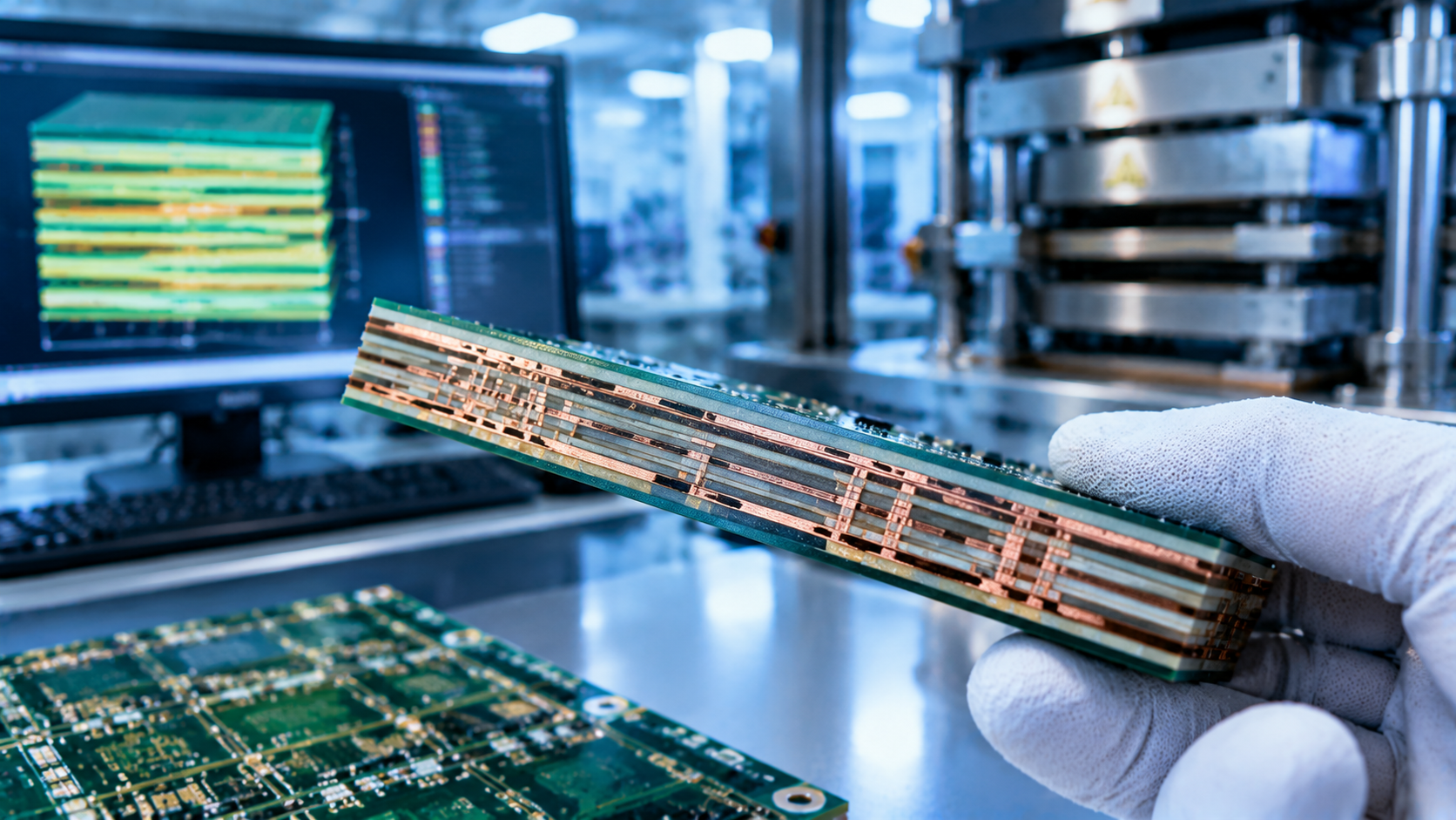
A PCB stack-up determines signal integrity, power integrity, EMI/EMC performance, and manufacturing cost. When designing boards with four or more layers, stack-up decisions directly impact board performance and price. This guide covers stack-up fundamentals, key design principles, and how stack-up choices affect circuit performance.
2026.10.26

Differential Pair Routing in PCB Design: Principles, Benefits, and Manufacturing Control

Differential pair routing is the standard for high-speed signals like PCIe, USB, HDMI, and Ethernet. This guide covers the two core principles—length matching and width matching—along with six key benefits including strong noise immunity, EMI suppression, and lower power consumption. It also explains how manufacturing controls differential impedance in production.
2026.10.23

How to Inspect PCB Laser Solder Joints: 4 Optical Detection Methods

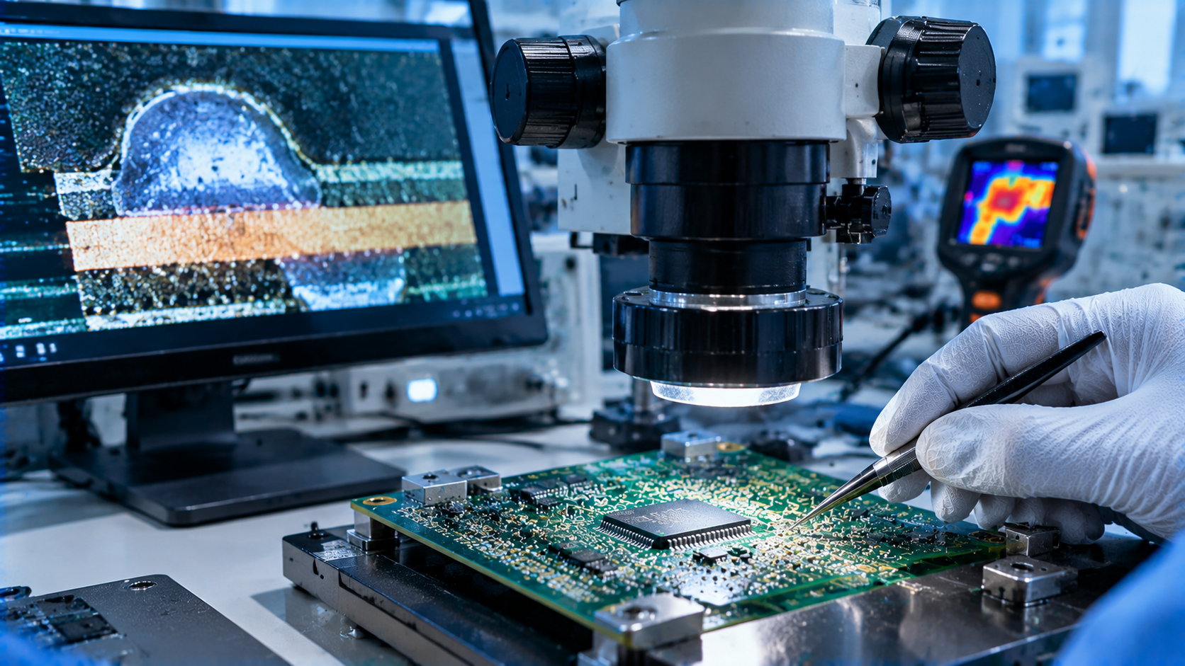
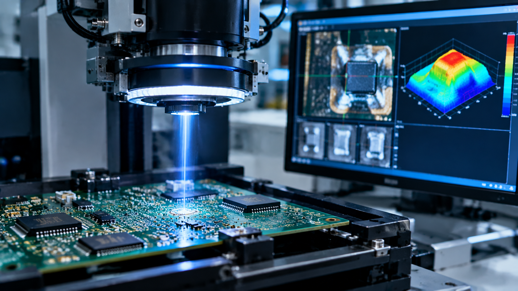
As electronics move toward miniaturization, laser solder joints are becoming smaller and harder to inspect. This guide covers four optical detection methods used to evaluate solder joint quality—laser triangulation, reflection distribution, multi-angle imaging, and multi-focus detection—and explains how process control from SPI to 3D AOI prevents defects at the source.
2026.10.22

Why AOI Inspection Is the Gatekeeper of SMT Solder Quality

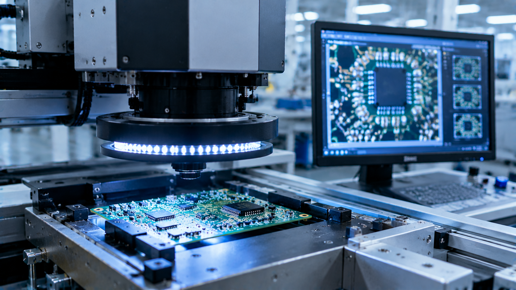
As PCBs shrink and component density increases, manual visual inspection is no longer enough. AOI (Automated Optical Inspection) uses high-resolution cameras and image processing to catch missing components, misalignments, and solder defects right on the SMT line. This guide covers how AOI works, what it can detect, and how manufacturing process control prevents the most common SMT defects.
2026.10.21

Power PCB Design Essentials: From Thermal Management to Manufacturability

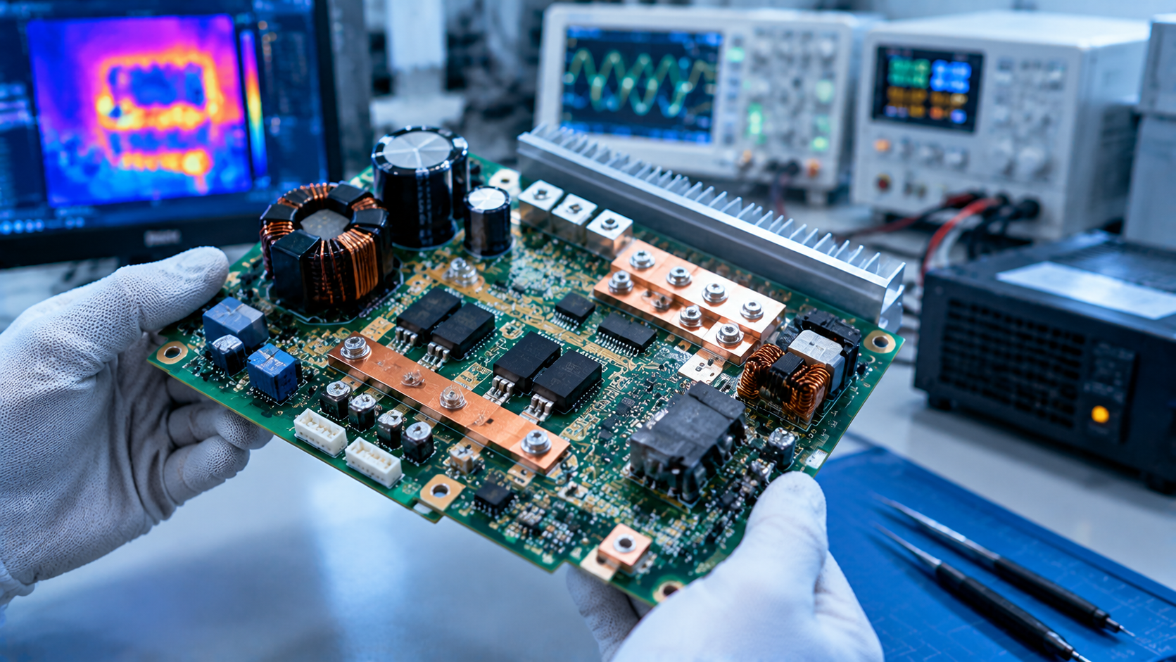
Power PCBs face challenges that standard signal boards don't: high currents, high voltages, and extreme heat. This guide covers the core essentials of power PCB design—thermal management, power and ground routing, component layout, via design, protection circuits, and EMC—while highlighting the manufacturing pitfalls that can cause production failures.
2026.10.21