Choosing a High-Quality PCB Manufacturer: A Comprehensive Guide
In today's world of technological advancement, printed circuit boards (PCBs) are at the heart of almost every electronic device, from smartphones to spacecraft. The quality of these boards directly impacts the performance and reliability of the final product. Choosing the right high quality PCB manufacturer is essential for success. This article will guide you through key considerations when selecting a PCB manufacturer, reviewing top players in the industry, and ensuring your project benefits from top-tier PCB fabrication.
Key Factors to Consider When Selecting a High-Quality PCB Manufacturer
Selecting a high-quality PCB manufacturer is crucial for the success of any electronics project. This decision requires a thorough evaluation of several critical factors that directly impact the final product's performance, reliability, and cost. These considerations range from the manufacturer's technical capabilities to their adherence to quality standards.
- Manufacturing Capabilities
Assess the manufacturer's ability to produce the specific type of PCBs required, including layer count, board thickness, and minimum trace width/spacing. Advanced capabilities like HDI (High-Density Interconnect) and microvias are crucial for complex designs. - Material Options
Evaluate the range of materials offered, such as FR-4, Rogers, and metal core substrates. The choice of material affects thermal, electrical, and mechanical properties and should align with the application requirements. - Quality Control Processes
Inquire about the manufacturer's quality control measures throughout the production process. This includes inspections at various stages, electrical testing, and functional testing to ensure the boards meet required standards. - Certifications and Compliance
Confirm that the manufacturer holds relevant certifications like ISO 9001, UL, and IPC standards. These certifications guarantee that they follow rigorous quality management and manufacturing processes. - Production Capacity
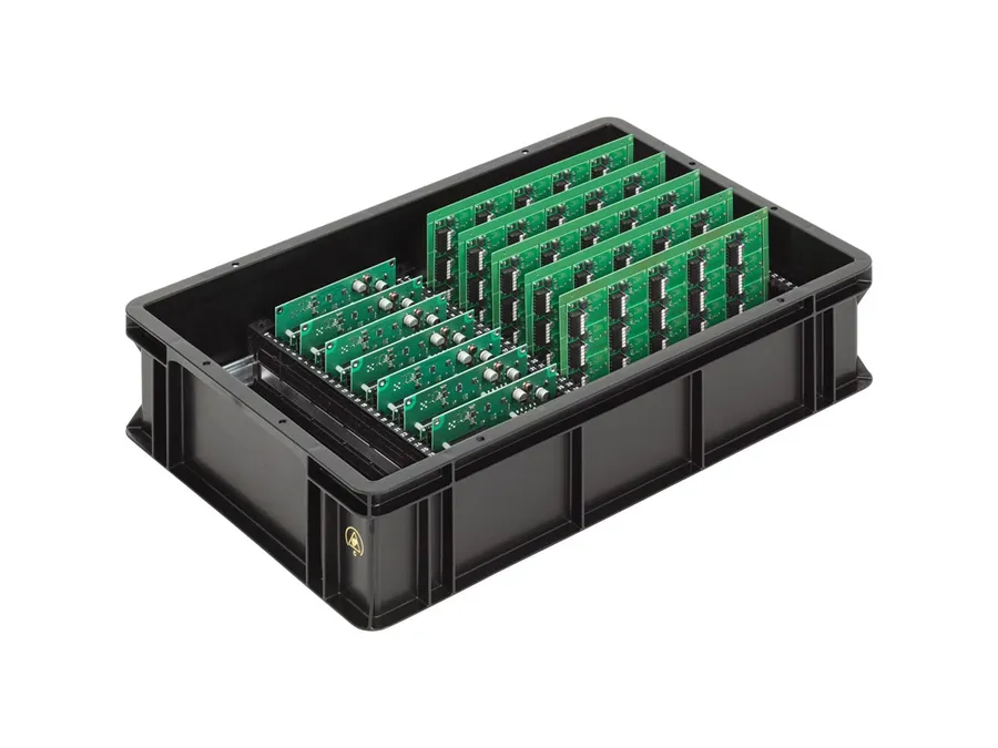
Consider the manufacturer's production capacity to meet the required volumes and timelines. It's essential to ensure they can handle your project's scale without delays. - Turnaround Time
Evaluate the typical turnaround times for both prototype and production quantities. Faster turnaround is essential for time-sensitive projects. - Cost Analysis
Analyze the overall cost, considering not only the unit price but also tooling costs, shipping expenses, and any potential hidden fees. Balancing quality with cost is vital for a successful project.
Understanding PCB Manufacturing Processes and Technologies
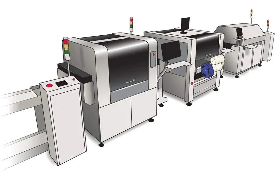
The fabrication of printed circuit boards (PCBs) involves a diverse array of processes and technologies, each contributing to the final product's functionality and reliability. These processes range from basic single-layer board production to complex multilayer and flexible circuit fabrication, catering to a broad spectrum of electronic applications.
Understanding the nuances of each process is crucial for engineers and designers to ensure the selected manufacturing approach aligns with their project's specific requirements, performance goals and cost constraints. The choice of technology impacts not just the final board's functionality but also its overall cost and reliability. This section will explore several key PCB manufacturing methods, their underlying technologies, and the associated trade-offs.
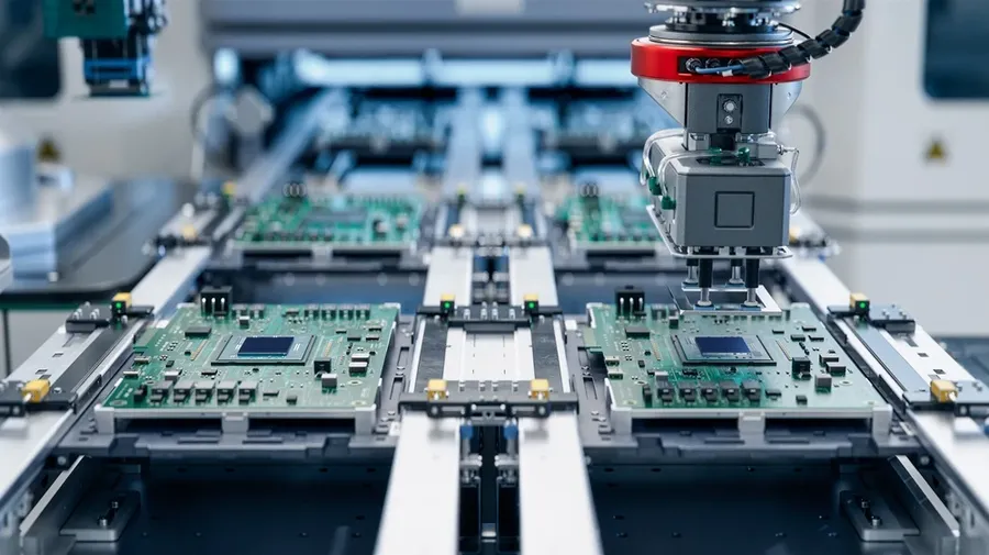
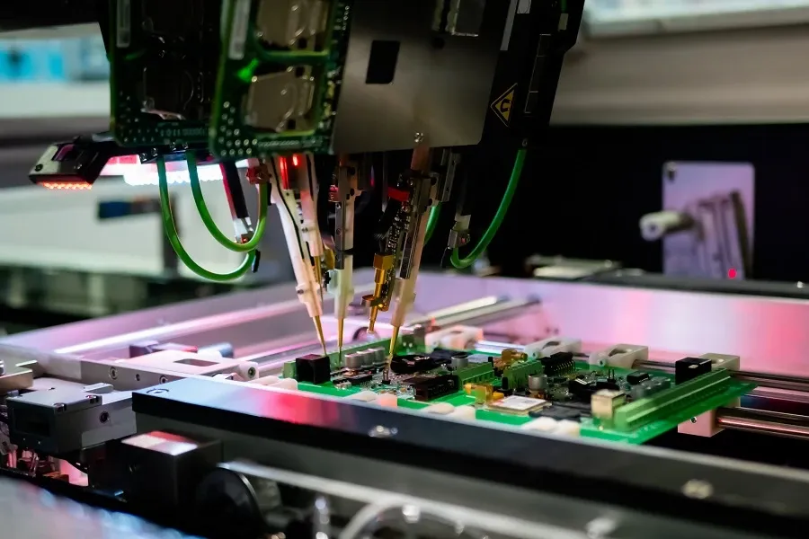
- Surface Mount Technology (SMT)
SMT involves mounting electronic components directly onto the surface of the PCB, rather than through holes. This method enables higher component density and faster assembly speeds, which are crucial for modern electronics. SMT is preferred for its efficiency and suitability for miniaturized devices, and it can accommodate a wide variety of component types, including surface-mount resistors, capacitors, and ICs. It is the dominant assembly method used in most modern electronic devices. - Through-Hole Technology
Through-hole technology involves inserting component leads into drilled holes on the PCB and soldering them on the opposite side. While it is less common in mass-produced electronics, through-hole technology provides strong mechanical bonds, making it suitable for applications requiring high reliability and robustness. It is particularly relevant for components that need physical support, such as large connectors and power components that might be subjected to stress. - Multilayer PCB Fabrication
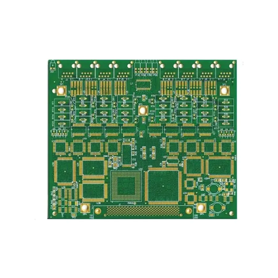
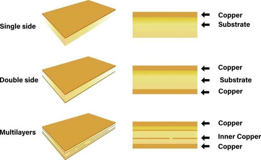
Multilayer PCBs are constructed by stacking multiple layers of copper traces, typically separated by an insulating material such as prepreg. These layers are interconnected through vias (plated through holes), enabling complex routing and signal transmission within the board. Multilayer designs are essential for creating high-density circuits with optimized signal integrity, which makes them ideal for complex electronic devices. The number of layers can range from 4 to over 40, depending on the complexity of the design. - High-Density Interconnect (HDI) PCBs
HDI PCBs are characterized by their high wiring density per unit area. These boards use microvias, fine lines, and small spacing to achieve miniaturization and improved performance. HDI technology enables complex, high-performance designs in very compact form factors, making it indispensable for advanced electronic applications like smartphones, tablets, and medical devices. HDI boards are significantly more complex and expensive to manufacture but can provide dramatic improvements in performance and size. - Flexible PCBs (Flex PCBs)
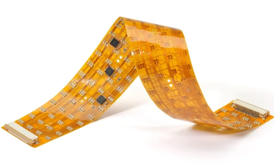
Flex PCBs utilize flexible substrate materials, such as polyimide, allowing the circuit board to bend and flex without breaking. This makes them ideal for dynamic applications where flexibility and space-saving are required. Flex PCBs are often used in compact consumer electronics, automotive applications, medical devices and aerospace applications, where they can fit into tight spaces and withstand vibrations.
A Comparison of Top PCB Manufacturers
Selecting the right PCB manufacturer is crucial for ensuring the success of any electronics project. This section provides an analytical comparison of leading PCB manufacturers, highlighting their unique specializations, strengths, and weaknesses. We will delve into crucial aspects such as manufacturing quality, production costs, and turnaround times to help you make an informed decision.
| Manufacturer | Specialization | Strengths | Weaknesses | Typical Lead Time | Cost Level |
|---|---|---|---|---|---|
| PCBWay | Prototyping and Small-Batch Production | Wide range of services, good online platform, quick turnaround for prototypes | Quality can vary, not the best for extremely high-end applications | 2-7 days for prototypes | Low to Mid-range |
| JLCPCB | Low-Cost Prototyping | Very affordable, efficient ordering process, good for simple PCBs | Limited material options, quality consistency can be an issue for complex boards | 3-10 days for prototypes | Low |
| Advanced Circuits | High-Reliability PCBs, Advanced Technologies | High-quality manufacturing, advanced capabilities (HDI, flex), good customer support | More expensive than budget options, not ideal for simple or low cost projects | 5-15 days | Mid to High-range |
| Sunstone Circuits | Fast Turn Prototyping, High Quality | Excellent customer service, good for complex designs, fast turnaround options | Higher cost, limited material selection, not ideal for very low cost projects | 3-10 days | Mid to High-range |
PCB Material Selection: Impact on Performance and Cost
The selection of PCB materials is paramount to the overall performance, reliability, and cost-effectiveness of the final product. Different materials exhibit distinct thermal, electrical, and mechanical properties, which directly influence the functionality and longevity of the printed circuit board. This section will explore the critical aspects of material selection, guiding engineers and designers toward making informed decisions tailored to their specific application requirements.
| Material | Dielectric Constant (εr) | Thermal Conductivity (W/m·K) | Glass Transition Temperature (Tg) | Typical Applications | Cost |
|---|---|---|---|---|---|
| FR-4 | 4.2-4.8 | 0.2-0.3 | 130-180 °C | General-purpose PCBs, Consumer electronics | Low |
| Rogers 4350B | 3.66 | 0.62 | 280 °C | RF and microwave applications, High-speed digital circuits | High |
| Rogers 4003C | 3.55 | 0.68 | 280 °C | High-frequency applications, Wireless communication | High |
| Metal Core (Aluminum) | N/A (Substrate is conductive) | 200-237 | N/A | LED lighting, Power electronics, High thermal dissipation applications | Medium to High |
| Polyimide | 3.2-3.5 | 0.3-0.4 | 250-300 °C | Flexible PCBs, High-temperature environments, Aerospace applications | Medium to High |
- FR-4 (Flame Retardant 4):
The most commonly used material due to its balance of performance, cost, and availability. It is a glass-reinforced epoxy laminate, suitable for a wide range of applications but may not be ideal for high-frequency or high-temperature environments. - Rogers Materials (e.g., 4350B, 4003C):
Specialty materials with superior electrical properties, often employed in RF, microwave, and high-speed digital applications. They exhibit lower dielectric loss and a more stable dielectric constant over frequency and temperature, but typically come at a higher cost than FR-4. - Metal Core PCBs (MCPCBs):
These use a metal base (typically aluminum) for enhanced thermal management. Ideal for high-power applications where heat dissipation is critical, such as LED lighting and power electronics. - Polyimide:
Used in flexible PCBs due to their excellent flexibility and high-temperature resistance. Suitable for dynamic bending or harsh environmental conditions.
The dielectric constant (εr) of the material directly affects the impedance of the traces, which is crucial for signal integrity, especially in high-speed circuits. Thermal conductivity influences how effectively heat is dissipated, impacting the reliability and performance of heat-generating components. The glass transition temperature (Tg) defines the temperature at which the material's properties change significantly, limiting operational environments. Careful consideration of these factors is essential to select the correct PCB material that meets the application requirements of performance and cost.
Quality Assurance and Testing in PCB Manufacturing
Rigorous quality assurance and testing are paramount in PCB manufacturing to ensure the reliability and performance of the final product. This involves comprehensive inspections, electrical testing, and adherence to strict industry standards, all aimed at identifying and rectifying defects at every stage of the production process. This commitment to quality is a critical differentiator for high-quality PCB manufacturers.
- Incoming Material Inspection (IQC)
This initial inspection verifies that all raw materials, such as laminates, copper foils, and soldermask, meet the specified quality standards before they are used in production. This includes checking for dimensional accuracy, material composition, and surface finish. - In-Process Quality Control (IPQC)
Implemented throughout the manufacturing process, IPQC includes visual inspections of the PCB layers, drilling accuracy, plating thickness, and etching quality. This ensures each step is completed correctly before moving to the next. - Automated Optical Inspection (AOI)
AOI systems use high-resolution cameras to capture images of PCBs and compare them with the design data. These systems can quickly identify defects such as shorts, opens, missing pads, and other irregularities that are difficult to detect with the naked eye. - Electrical Testing
Electrical tests verify the functionality of the PCB by measuring the conductivity between various points on the board. This typically includes continuity tests (to ensure that traces are correctly connected) and isolation tests (to check for shorts). Electrical tests include: flying probe testing, bed-of-nails testing, or other methods. - Functional Testing (FCT)
This is the final quality check, where the assembled PCB is tested under simulated operating conditions. Functional testing confirms that the PCB is performing as intended and verifies the functionality of all components. - Final Visual Inspection
Before packaging, PCBs undergo a final visual inspection to detect any remaining defects or cosmetic imperfections that may have been missed in previous inspections. This includes checking for solder joint quality, component placement, and overall cleanliness.
Certifications and standards play a vital role in ensuring PCB quality. Key certifications include ISO 9001 (Quality Management Systems), ISO 13485 (Medical Devices), and UL certifications. Compliance with industry standards, such as IPC standards (especially IPC-A-600 for PCB acceptance criteria), demonstrates a commitment to producing high-quality PCBs and is an important indicator of a reliable high quality pcb manufacturer.
Geographic Considerations When Choosing a PCB Manufacturer
Selecting a PCB manufacturer involves a critical decision regarding geographic location, as domestic and international options present distinct advantages and disadvantages. These choices impact lead times, shipping costs, communication efficacy, and intellectual property protection, significantly influencing the overall project timeline and budget.
| Factor | Domestic Manufacturers | International Manufacturers |
|---|---|---|
| Lead Times | Generally shorter due to proximity and streamlined logistics. | Often longer due to shipping distances and potential customs delays. |
| Shipping Costs | Lower shipping expenses due to shorter transportation distances. | Higher shipping costs due to international shipping and potential import duties. |
| Communication | Facilitated by similar time zones and language, enhancing clarity and reducing misunderstandings. | Can face communication barriers due to time zone differences and potential language variations. |
| Quality Control | Easier to conduct on-site audits and maintain close oversight on manufacturing processes. | Quality oversight may be more challenging due to geographical distance. |
| Intellectual Property Protection | Generally stronger legal frameworks for intellectual property protection. | IP protection can be riskier due to varying legal systems and enforcement. |
| Cost | Higher production cost due to labor costs, overheads and other factors. | Lower production cost due to lower labor costs and lower material costs. |
| Response Time | Faster response time in case of inquiries, issue resolution and engineering changes. | Slower response time due to time zone differences and communication barriers. |
Choosing between domestic and international PCB manufacturers requires a careful evaluation of these tradeoffs, tailored to the specific project requirements, budget, and timeline. For high-complexity, high-reliability applications where speed, quality, and intellectual property are critical, domestic options may be preferred despite the higher cost. Conversely, for high volume and lower cost projects, international options may be a better fit.
Frequently Asked Questions about High-Quality PCB Manufacturers
Selecting the right PCB manufacturer can be complex. This section addresses common questions to clarify key aspects of PCB manufacturing, aiding in informed decision-making.
- What are typical minimum order quantities (MOQs) for PCBs?
MOQs vary significantly between manufacturers. Some, especially those focusing on prototyping, may offer very low MOQs, even single boards. Others, particularly larger-scale manufacturers, may have MOQs ranging from 5 to 100 or even more. It’s essential to check with each manufacturer to understand their specific requirements. - What is 'Design for Manufacturing' (DFM) and why is it important?
DFM is the process of designing PCBs with manufacturing efficiency in mind. Following DFM guidelines prevents errors in production, reduces cost and waste, and speeds up manufacturing. This includes considerations such as trace widths and spacing, pad sizes, via placement, and component orientations. It's crucial for reducing delays and ensuring manufacturability. - How does the PCB quoting process typically work?
The quoting process usually begins with providing the manufacturer with Gerber files, a bill of materials (BOM), and any special requirements. Manufacturers use this data to evaluate the complexity of the design, the material needs, and the production volume to generate a price quote. Factors affecting the quote include layer count, board size, material type, surface finish, quantity, and turnaround time. Always compare quotes from multiple manufacturers to ensure a competitive price. - What are typical lead times for PCB manufacturing?
Lead times vary depending on the complexity of the PCB, the manufacturer’s workload, and the manufacturing location. Simple prototype boards can have lead times of a few days to a week. More complex multilayer boards can take several weeks or more, especially with overseas manufacturing. Always verify lead times when placing the order and ensure they are compatible with your project timeline. Some manufacturers offer expedited services for an additional fee. - What types of PCB testing are typically performed by manufacturers?
Manufacturers use several tests to ensure the quality of the manufactured boards. These may include visual inspection, automated optical inspection (AOI), in-circuit testing (ICT) which tests for shorts or opens, and flying probe tests. High-quality manufacturers provide electrical testing to ensure the functionality of the boards based on your specifications, with final functional tests to verify the boards perform as intended. - How do I choose between domestic and international PCB manufacturers?
Domestic PCB manufacturers often offer faster lead times and better communication due to closer proximity. However, they may have higher costs than international manufacturers. International manufacturers can be very cost-effective, particularly for large quantities, but they may have longer lead times, potential communication barriers, and additional shipping costs and considerations. The choice depends on your specific needs, project budget and timeline. - What are the key factors to consider when comparing PCB manufacturers?
When comparing manufacturers, consider factors including manufacturing capabilities (layer count, materials, tolerances, technologies), quality control processes, certifications (ISO, UL), customer support, pricing, and lead times. Also check for reviews or ask for customer references. Match these factors against your project's requirements to choose the manufacturer that is best for your needs.
Cost-Effective Strategies for PCB Manufacturing
Optimizing PCB designs for cost-effectiveness is crucial for reducing manufacturing expenses without compromising quality. Several strategies can be employed, focusing on design choices and material considerations to minimize waste and simplify production.
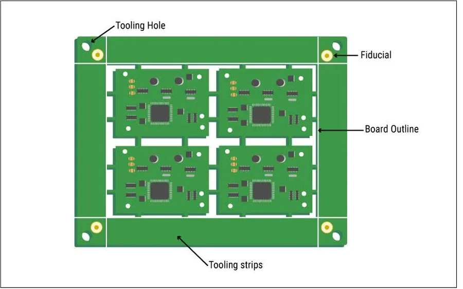
- Panelization
Panelizing your PCB design involves combining multiple individual boards into a larger panel. This allows for more efficient use of manufacturing materials and equipment, reducing overall costs. Manufacturers can process larger volumes simultaneously, decreasing per-unit costs. However, consider the complexity of depanelization which may impact the overall cost - Component Selection
Choosing standard, readily available components reduces procurement costs and lead times. Opting for cost-effective alternatives that meet the functional requirements without over-specifying can also lead to significant savings. Consider also the long-term availability of components to avoid costly redesigns. - Standard Layer Stackups
Using standard layer stack-ups reduces complexity in manufacturing which leads to lower prices and faster delivery times. Non-standard stackups will require more preperation time and costs of setup. Design your boards with material thicknesses and copper weights commonly used. - Streamlined Layout Techniques
Efficient component placement and routing minimize the amount of PCB real estate required, resulting in lower material costs. Utilizing simpler trace designs, and wider traces (when possible) reduces etching and fabrication complexity. Utilizing via-in-pad technologies for surface mount components can also save board space and reduce layer counts. - Design for Manufacturability (DFM)
Early engagement with your manufacturer to ensure your design is compatible with their processes is critical. Addressing any potential issues at the design stage avoids costly revisions and scrap. Adhering to the manufactures prefered design rules will reduce costs and prevent production delays. - Optimize Trace Width and Spacing
Using the largest trace width and spacing possible that meets the design criteria can help reduce etching costs and production difficulties. Smaller traces require greater accuracy and control in the etching and fabrication steps. - Minimize the Number of Layers
Reducing the number of layers in a PCB design can greatly lower costs. This usually can be done through careful component placement, trace routing, and the use of surface mount components. While a design may need a large number of layers in some situations, optimizing component placement and routing to avoid the need for higher layer counts can save significant cost.
Future Trends in PCB Manufacturing
The printed circuit board (PCB) manufacturing sector is undergoing a significant transformation driven by technological advancements and evolving market demands. Emerging trends like additive manufacturing, sustainable practices, and the integration of advanced materials are poised to redefine how PCBs are designed, produced, and utilized, leading to greater efficiency, enhanced performance, and reduced environmental impact.
- Additive Manufacturing (3D Printing)
Additive manufacturing, or 3D printing, is revolutionizing PCB production by enabling the creation of complex geometries and customized designs layer by layer, thus reducing material waste, shortening prototyping time, and allowing for the production of PCBs with unique shapes and integrated components. - Sustainable Practices
The push for sustainability is reshaping PCB manufacturing, leading to the adoption of eco-friendly materials, waterless processing techniques, and closed-loop recycling systems to minimize environmental impact, conserve resources, and meet increasingly stringent environmental regulations. - Advanced Materials
Research into advanced materials is driving innovations in PCB fabrication by introducing substances with enhanced electrical, thermal, and mechanical properties. This includes materials like graphene, carbon nanotubes, and novel polymers that can enable higher performance, greater durability, and increased functionality in PCBs. - Integration of AI and Automation
The application of Artificial Intelligence (AI) and automation technologies in PCB manufacturing is optimizing process control, improving quality, and increasing efficiency by streamlining operations and enhancing predictive maintenance capabilities. - Embedded Components
Embedding components within the PCB substrate allows for miniaturization, improved electrical performance, and increased design flexibility. This trend is particularly relevant for high-density applications in consumer electronics, wearables, and other small form-factor products.
Selecting a high quality pcb manufacturer is a decision that impacts the entire life cycle of your product. By carefully assessing manufacturing capabilities, material choices, quality controls and geographic location, you can ensure that the PCBs meet the required standards and reliability for their intended applications. This approach will also enable you to make informed decisions on sourcing and production, ultimately contributing to the success of your electronic products. When choosing your manufacturer, remember to factor in reputation, responsiveness, and the ability to handle future needs to establish a long-term partnership with a reliable and high-quality pcb manufacturer.