Comprehensive Guide to PCB Manufacturing and Assembly
In our increasingly interconnected world, Printed Circuit Boards (PCBs) are the invisible backbone of almost every electronic device. From the smartphones we rely on to the intricate machinery that powers industries, PCBs are crucial. Understanding both PCB manufacturing and assembly is key for anyone involved in electronics development and production. This article serves as a comprehensive guide, detailing the nuances of each step, offering clarity, and helping you navigate the world of PCB creation effectively.
Understanding PCB Manufacturing: The Foundation
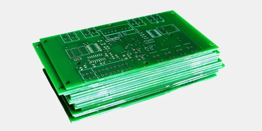
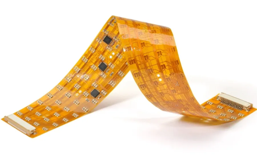
PCB manufacturing is the foundational process of creating the bare printed circuit board, transforming design specifications into a physical substrate ready for component assembly. This intricate process involves multiple stages, from selecting appropriate base materials to the final testing of the bare board, and requires precision and adherence to strict quality standards to ensure the functionality and reliability of the final electronic product. The process is distinct from PCB assembly, which involves adding electronic components to the manufactured board.
| Process Stage | Description |
|---|---|
| Substrate Selection | Choosing the base material, typically a composite like FR-4, based on thermal, mechanical, and electrical requirements. |
| Image Transfer | Transferring the circuit design onto the substrate using methods like photolithography, where a photosensitive material is exposed to UV light through a photomask. |
| Etching | Removing unwanted copper from the board using chemical etching processes, leaving only the desired circuit traces. |
| Layer Lamination | Pressing together multiple layers of PCBs in a multilayer board using heat and pressure to achieve the necessary copper trace connections and isolation. |
| Drilling | Creating holes in the PCB for component placement and electrical connections, employing precision drilling tools. |
| Plating | Applying a conductive coating to the drilled holes and surface to facilitate electrical connections |
| Solder Mask Application | Applying a solder mask, a protective layer that prevents solder bridges between traces, enhancing assembly process. |
| Silkscreen Printing | Printing component designators and logos on the board using silkscreen ink for easy identification during assembly and debugging. |
| Final Testing | Verifying the board's integrity and electrical connections through testing, including short and open circuit tests. |
PCB Assembly Process: Bringing Components Together
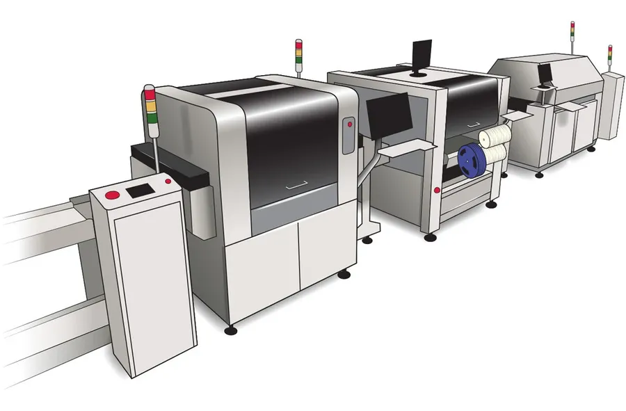
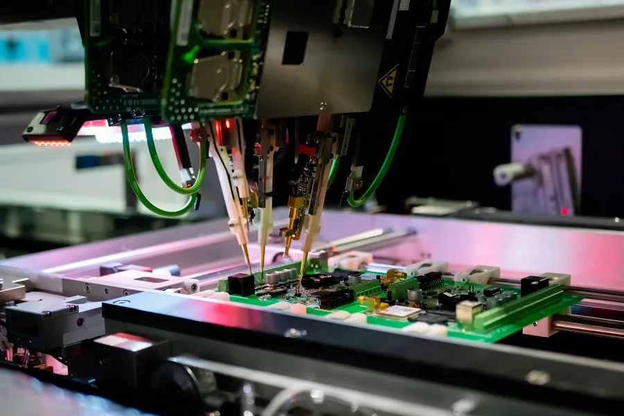
The PCB assembly process is the critical stage where electronic components are mounted onto a bare printed circuit board (PCB), transforming it into a functional electronic module. This process involves several intricate steps, from component placement to soldering and quality inspection, ensuring the final product meets design specifications and performance requirements. Key techniques include Surface Mount Technology (SMT), through-hole assembly, and manual assembly for specialized needs.
- Component Selection and Preparation
The process begins with the careful selection of electronic components based on the PCB design. These components are prepared for assembly, which may involve placing them in feeders for automated pick-and-place machines or preparing them manually for hand assembly. - Solder Paste Application
For SMT assembly, solder paste, a mixture of solder particles and flux, is precisely applied to the PCB pads using a stencil. This ensures that the solder is only applied where components will be placed. - Component Placement
Automated pick-and-place machines or manual placement is used to place components onto the PCB, accurately positioning them on the solder paste. SMT components are placed on the surface, while through-hole components are inserted through drilled holes in the board. - Reflow Soldering
The PCB is then passed through a reflow oven, where the solder paste is melted, creating a permanent electrical and mechanical connection between the components and the PCB. The temperature profile of the oven is carefully controlled to ensure proper solder joint formation and component integrity. - Through-Hole Soldering
For through-hole components, soldering is often performed manually or by wave soldering machines. Wave soldering involves passing the PCB over a wave of molten solder. - Automated Optical Inspection (AOI)
After soldering, AOI machines are used to detect any soldering defects, component placement issues, and other inconsistencies, ensuring a high quality standard. - Final Inspection and Testing
The assembled PCB undergoes a final inspection, which may include electrical testing, x-ray inspection, and functional testing to verify its performance and reliability.
| Assembly Technique | Description | Typical Application |
|---|---|---|
| Surface Mount Technology (SMT) | Components are mounted directly onto the surface of the PCB. | High volume manufacturing of consumer electronics. |
| Through-hole Technology | Components are inserted through drilled holes and soldered on the opposite side. | Applications requiring robust mechanical connections. |
| Hand Assembly | Components are manually placed and soldered onto the PCB. | Prototyping, low-volume orders, specialized components. |
| Wave Soldering | PCB passed over a wave of molten solder | Through-hole component soldering in high volume. |
Key Differences Between PCB Manufacturing and PCB Assembly
The core distinction between PCB manufacturing and PCB assembly lies in their respective focuses: manufacturing creates the bare circuit board, while assembly populates that board with electronic components. These two processes are sequentially dependent; the board must be manufactured before it can be assembled.
| Aspect | PCB Manufacturing | PCB Assembly |
|---|---|---|
| Primary Goal | Creation of the bare PCB | Population of the PCB with components |
| Input | PCB design files (e.g., Gerber files) | Bare PCB, Bill of Materials (BOM), component placement data |
| Key Processes | Substrate selection, Image transfer, Etching, Drilling, Plating, Solder mask application | Component sourcing, Solder paste application, Component placement (SMT & Through-hole), Reflow soldering, Wave soldering, AOI, Functional testing |
| Output | Bare printed circuit board | Fully populated PCB assembly |
| Interdependence | Independent Process with dependent on PCB design | Dependent on PCB manufacturing |
Cost Factors in PCB Manufacturing and Assembly
The cost of PCB manufacturing and assembly is influenced by a multitude of factors, each playing a significant role in the final price. Understanding these factors is crucial for cost optimization and effective budgeting. This section breaks down these variables, offering insight into how each one affects the overall expenditure.
| Cost Factor | Description | Impact on Cost |
|---|---|---|
| Material Selection | The type of substrate (e.g., FR-4, aluminum), copper thickness, and other materials used. | High-performance materials or unique substrates significantly increase cost. |
| Design Complexity | The number of layers, board dimensions, via density, trace width and spacing, and component footprint complexity. | More complex designs (e.g., high layer count) lead to increased manufacturing time and cost. |
| Quantity of Boards | The volume of PCBs produced in one order. | Larger quantities usually lead to lower per-unit cost due to economies of scale. |
| Lead Times | The time required for manufacturing and assembly. | Expedited lead times (rush orders) typically incur higher costs. |
| Component Sourcing | The cost of electronic components and how they are sourced. | Components with long lead times, rare, or from unofficial sources, increase total cost. |
| Assembly Method | Surface Mount Technology (SMT) vs. Through-Hole Technology (THT), manual vs. automated | Automated assembly with SMT is generally more cost-effective for higher volumes. |
| Testing Requirements | The depth and type of tests required (e.g., electrical tests, AOI, functional tests). | More rigorous testing can add to the overall cost. |
| Surface Finish | The type of surface plating (e.g., HASL, ENIG, Immersion Silver). | Finishes like ENIG are more expensive than HASL. |
To optimize costs, consider these tips: 1. Design for manufacturability (DFM): Simplify your PCB design by adhering to standard trace widths, clearances, and component footprints, reducing production complexities. 2. Optimize board size: Minimize the board dimensions to save on material and production expenses. 3. Standardize component selection: Select readily available and reasonably priced electronic components. 4. Plan for volume: If future demand allows, increase the batch quantity to benefit from economies of scale. 5. Plan your lead times realistically: Avoid rush orders by planning well in advance. 6. Evaluate surface finishes: Choose surface finishes appropriate for your project requirements, potentially avoiding more costly options where they are not necessary.
Choosing the Right PCB Manufacturing and Assembly Services

Selecting the ideal PCB manufacturing and assembly service is critical for project success, directly impacting quality, cost, and timelines. This section provides a framework for evaluating providers, emphasizing expertise, technology, certification, lead times, and support.
When selecting a PCB manufacturing and assembly service provider, consider the following criteria, ensuring they align with your project's requirements and constraints:
- Technical Expertise and Experience
Assess the provider's track record and experience, particularly with projects similar to your own. A seasoned provider will have a deeper understanding of potential issues and offer robust solutions. - Technological Capabilities
Evaluate the technologies offered, encompassing SMT and through-hole capabilities, and their capacity to handle complex PCB designs. The technology should be adequate to meet current needs and scalable to future requirements. - Quality Certifications
Confirm the presence of relevant certifications, such as ISO 9001 or IPC standards. These accreditations validate the provider's adherence to quality management principles. - Turnaround Time and Lead Times
Evaluate the provider's ability to meet your time constraints, from prototype development to mass production, and their response to expedited requests. - Customer Support and Communication
Assess their communication effectiveness, responsiveness to queries, and proactive approach to addressing concerns, all critical for a smooth collaborative process. - Pricing and Transparency
Compare quotes from different suppliers ensuring that these quotes are transparent, detailing costs for each process, including PCB manufacturing, component sourcing, and assembly. - Component Sourcing Capabilities
If the provider offers component sourcing, evaluate their supply chain network to ensure that they have the capacity to source quality components from reliable distributors and at reasonable costs. - Online Quoting and Turnkey Solutions
Check for user-friendly online quoting tools for ease of cost assessment, and turnkey options for simplified project management. These features can greatly reduce the overall project cycle time.
By carefully considering these criteria, you can select a PCB manufacturing and assembly partner that best aligns with your specific project needs, reducing the risk of delays and quality issues while ensuring cost-effectiveness.
PCB Manufacturing and Assembly: Quality Control and Testing
Rigorous quality control and testing are paramount in both PCB manufacturing and assembly to ensure the reliability and functionality of the final product. These measures span from the bare board production to the fully assembled PCB, encompassing electrical, visual, and functional assessments.
The purpose of quality control is to identify defects early in the process, which reduces the cost and effort to fix these issues later on, and ensures the PCBs meet required standards.
| Test Type | Description | Purpose | Stage |
|---|---|---|---|
| Electrical Tests | Continuity tests to verify the connections, Impedance testing and shorts detection. | Ensures signal integrity and proper function, prevents short circuits. | Bare board & assembled board |
| X-Ray Inspection | Non-destructive testing, using x-rays, to check the interior of the PCB for defects. | Identifies hidden defects such as solder voids, misaligned components, and shorts in BGAs or other complex packages. | Assembled board |
| Automated Optical Inspection (AOI) | Automated visual inspection to check for component placement, soldering quality, and other visible defects. | Ensures accuracy and reduces manual inspection time. | Assembled board |
| Functional Testing | Verifies the functional performance of the assembled PCB, often using test jigs and fixtures, simulating real operational conditions. | Confirm the operation of the board according to it's intended purpose and find out any failure modes before releasing to clients. | Assembled board |
| Visual Inspection | A basic but crucial test where boards are checked visually for any defects such as scratches or misalignments. | Identifies physical defects that could affect performance | Bare board & assembled board |
Frequently Asked Questions About PCB Manufacturing and Assembly
This section addresses common inquiries regarding PCB manufacturing and assembly, providing clear and concise answers to help clarify the processes involved.
- What is the fundamental difference between PCB manufacturing and assembly?
PCB manufacturing, also known as fabrication, focuses on creating the bare printed circuit board. This involves processes like etching, drilling, and plating to form the conductive pathways on the substrate. PCB assembly, conversely, involves populating the manufactured board with electronic components, like resistors, capacitors, and integrated circuits, using techniques such as soldering. - Could you describe the typical PCB manufacturing process?
The PCB manufacturing process generally includes several key steps: design and layout using CAD software, printing the design onto a substrate, etching away unwanted copper, drilling holes for components and vias, plating the conductive surfaces, and finally, applying solder mask and silkscreen. This culminates in a bare board ready for assembly. - What are the main cost drivers in PCB assembly?
Several factors impact PCB assembly costs. These include the type and quantity of components, the complexity of the board design (number of layers, component density), the type of assembly technology used (SMT, through-hole, mixed), the required turnaround time, and the volume of boards. Material costs for solder and components, as well as labor costs for assembly, are also significant contributors. - Is PCB fabrication the same as PCB manufacturing?
While the terms are often used interchangeably, PCB fabrication is generally considered a subset of manufacturing that deals specifically with the bare board creation. So, PCB manufacturing is the umbrella term that can include both the bare PCB fabrication and the downstream PCB assembly processes. - What is the role of automated optical inspection (AOI) in PCB assembly?
Automated optical inspection (AOI) is a critical quality control step in PCB assembly. It uses a camera system to compare the assembled board against a reference design. AOI detects errors such as incorrect component placement, solder defects, and missing components, ensuring the quality and reliability of assembled boards. - What are some options for prototyping and low-volume PCB assembly?
For prototyping and low-volume orders, options include hand assembly and semi-automated methods. Some companies specialize in quick-turn services that can provide assembled prototypes within a short timeframe. There are also online PCB assembly service companies that allow engineers to upload a design and have small quantities assembled quickly. These options help iterate on designs cost-effectively before scaling up to large production volumes. - What are the key considerations when choosing a PCB manufacturer?
Selecting a PCB manufacturer requires careful consideration of several factors. These include the manufacturer's experience, technology capabilities, adherence to industry standards and certifications, quality control processes, material options, lead times, pricing structure, and customer service. It is beneficial to have clear communication and transparency throughout the entire process to ensure a smooth experience.
Trends and Innovations in PCB Manufacturing and Assembly
The PCB manufacturing and assembly landscape is continually evolving, driven by demands for increased functionality, miniaturization, and sustainability. These trends and innovations are shaping the future of electronics, demanding that manufacturers adapt to remain competitive. Understanding these advancements is crucial for businesses and engineers alike, enabling them to anticipate future requirements and optimize their processes.
- Advanced Materials
The development of new substrate materials with enhanced thermal and electrical properties are pivotal. These include materials such as advanced ceramics and polymers, enabling PCBs to operate in more extreme environments, offering improved signal integrity, and facilitating higher frequency operations. This is especially crucial for high-speed digital and RF circuits. - Miniaturization and High-Density Interconnect (HDI)
The push for smaller, more compact electronic devices requires PCB technology to shrink in size while increasing functionality. HDI technology, including microvias, fine-line traces, and blind/buried vias, allows for denser component placement and complex routing, optimizing space and performance in smaller form factors. This is essential for consumer electronics, medical devices, and IoT applications. - Additive Manufacturing (3D Printing)
Additive manufacturing, or 3D printing, is emerging as a transformative technique in PCB fabrication. This enables rapid prototyping and the creation of complex, non-planar board shapes, which is impossible with traditional subtractive methods. This technology reduces lead times, lowers production costs for small batches, and opens doors for new PCB designs with embedded components. - Sustainable and Environmentally Friendly Processes
Environmental concerns are driving the adoption of more sustainable practices in PCB manufacturing and assembly. This includes the use of lead-free solder, water-based or bio-based etching and cleaning solutions, and recycling initiatives for PCB waste. This reduces the industry's environmental impact and ensures compliance with regulations, while also improving the long term viability of the process. - Automated Assembly and Robotics
Increased automation and robotics in PCB assembly is essential for greater efficiency, precision, and speed. Automated pick-and-place machines, solder paste application systems, and reflow ovens, coupled with automated optical inspection (AOI), increase production throughput while enhancing the accuracy and consistency of the assembly process. This is vital for high-volume production and reducing human error. - Smart Factories and Industry 4.0 Integration
The integration of smart factory concepts, such as the use of big data, real-time monitoring, and AI, allows for better process control, predictive maintenance, and optimization of the entire production process. This results in improved efficiency, reduced defects, and faster cycle times, leading to higher quality PCBs and greater profitability for manufacturers. - Advanced Testing and Inspection Methods
Emerging testing and inspection techniques, such as X-ray laminography and advanced in-circuit testing (ICT), ensure the integrity and reliability of PCBs. These sophisticated methods are capable of detecting hidden defects, voids, and solder joint issues, thereby improving overall product quality. These techniques play an ever more important role due to the higher density interconnects.
Understanding PCB manufacturing and assembly is critical for creating high-quality, functional electronic products. Whether you need a quick PCB prototype or a large-scale production run, mastering these two processes helps ensure cost-effectiveness and reliability. As technology continues to advance, the processes involved in both PCB manufacturing and assembly will continue to evolve, making it essential to stay informed and adaptable. By embracing new techniques and maintaining a focus on quality, you can leverage the full potential of PCB technology in various applications.