Choosing the Right 16 Layer PCB Manufacturer: A Comprehensive Guide
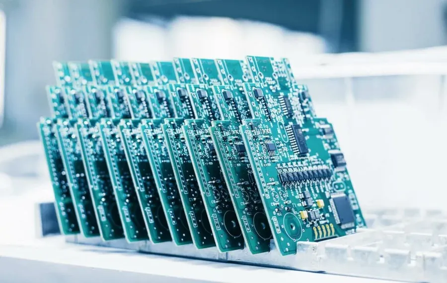
In today's ever-evolving landscape of electronic innovation, multilayer PCBs are the unsung heroes powering advancements across industries. Among these, 16 layer PCBs stand out as essential components in sophisticated devices and high-performance systems. Selecting the right 16 layer PCB manufacturer is crucial. Like choosing the right ingredients for a gourmet meal, partnering with a skilled and experienced PCB manufacturer ensures quality, reliability, and success in your project. This article will provide a comprehensive guide to what to look for to ensure you choose the ideal manufacturing partner and provides a wealth of actionable information to help you make the most informed decision.
Understanding the Need for 16 Layer PCBs
16-layer PCBs are a sophisticated solution for complex electronic designs requiring high circuit density, intricate signal routing, and superior performance, particularly in high-speed applications. These boards serve as the foundation for advanced electronic systems across various industries where performance and reliability are paramount.
The demand for 16-layer PCBs arises from several key factors. Firstly, their increased layer count allows for significantly higher circuit density compared to lower-layer PCBs. This is crucial in compact devices where space is limited but functionality must be maintained. Secondly, 16-layer PCBs facilitate complex signal routing with dedicated layers for power, ground, and signal, minimizing interference and signal degradation. This is especially important in high-speed digital and RF circuits where signal integrity is critical. Finally, these multilayer PCBs offer superior electrical and thermal performance, enabling them to function reliably in demanding environments.
Several industries rely heavily on the capabilities of 16-layer PCBs. These include, but are not limited to, telecommunications, where these PCBs are vital for networking equipment, servers, and routers. High-performance computing applications such as advanced data processing systems, server motherboards, and graphics cards often employ 16-layer PCBs for their robust performance. In the field of aerospace and defense, they are found in complex avionic systems, radar equipment, and guidance systems. Lastly, the medical industry utilizes them in sophisticated diagnostic equipment, imaging devices, and patient monitoring systems, where performance and reliability are non-negotiable.
Key Considerations When Selecting a 16 Layer PCB Manufacturer
Selecting the right manufacturer for 16-layer PCBs is crucial for ensuring the success of complex electronic designs. This decision hinges on several key factors that directly impact the quality, reliability, and cost-effectiveness of the final product. A thorough evaluation of a manufacturer's capabilities is essential to mitigate risks and achieve optimal results.
- Expertise in Multilayer PCB Manufacturing
A manufacturer's experience with multilayer PCBs, specifically 16-layer designs, is paramount. This includes their proficiency in handling the complexities of lamination, drilling, and plating for high-density interconnects. Look for a track record of successful 16-layer PCB projects, showcasing their ability to manage the intricate processes involved. - Manufacturing Capacity and Technology
Assess the manufacturer's production capacity to meet your project's volume requirements and timelines. Evaluate their technology stack, which should include advanced equipment for precise drilling, accurate imaging, automated optical inspection (AOI), and X-ray inspection. These are critical for ensuring the quality of multilayer boards, specifically when dealing with complex features and tight tolerances. - Material Selection
The range of available materials, including FR-4, high-Tg materials, and other advanced substrates, should be considered. Ensure the manufacturer can procure and process the specific materials your design requires. The selection of the right material directly impacts the performance and reliability of the final product. - Quality Control Processes
Rigorous quality control processes are crucial for ensuring that the PCBs meet the design specifications and performance requirements. The manufacturer should have established procedures for testing and inspection throughout the production process, and hold certifications that demonstrates their committment to quality standards. - Cost and Turnaround Time
Evaluate the cost implications considering your desired quantity, design complexity, and material selection. Balance this with the anticipated lead times for production, particularly if your project has time constraints. Transparent pricing and realistic turnaround times are essential to ensure project feasibility and on-time delivery. - Communication and Support
Effective communication channels and technical support are essential for a smooth manufacturing process. Assess the manufacturer's responsiveness to inquiries, willingness to address design concerns, and ability to manage potential issues. Ensure they can provide design rule checks (DRC) and support throughout the manufacturing process.
The Importance of 16 Layer PCB Stack-Up
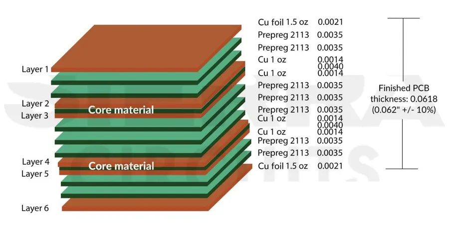
Proper 16-layer PCB stack-up is paramount for achieving optimal performance, signal integrity, and reliability in complex electronic devices. The arrangement of conductive and dielectric layers directly influences impedance control, signal quality, and thermal management, making it a critical aspect of PCB design.
A well-defined stack-up ensures controlled impedance, reducing signal reflections and ensuring that high-speed signals propagate efficiently. It also facilitates effective power distribution, thermal dissipation, and mitigates electromagnetic interference (EMI). Failing to address these aspects can result in signal degradation, unreliable performance, and reduced product lifespan.
| Layer | Function | Considerations |
|---|---|---|
| Signal Layers (multiple) | Routing of high-speed and low-speed signals | Trace width, spacing, and impedance control; proximity to ground/power layers |
| Ground Layers (multiple) | Reference planes for signals, EMI shielding, and heat dissipation | Continuous planes, minimizing discontinuities, connection to ground net |
| Power Layers (multiple) | Distribution of supply voltage(s) | Plane width for sufficient current carrying capacity, decoupling capacitors placement, minimal voltage drop |
| Dielectric Layers (multiple) | Insulation and separation of conductive layers | Material properties like dielectric constant, loss tangent and thickness impacting impedance and signal integrity |
Key considerations include the dielectric material (e.g., FR-4, high-Tg materials), the thickness of both dielectric and copper layers, and the sequence of signal, ground, and power planes. Different materials possess different dielectric constants and loss tangents, impacting impedance and signal integrity at high frequencies. Layer thickness dictates impedance and signal propagation speed.
A common 16-layer stack-up strategy involves alternating signal layers with ground and power planes to improve signal integrity, reduce crosstalk, and enhance power distribution. However, specific application requirements can influence this configuration. It is crucial to work closely with your chosen PCB manufacturer to choose the best stack-up for the specific needs of your design.
Materials and Finishes for 16 Layer PCBs
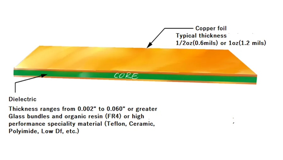
The selection of materials and surface finishes is crucial in the fabrication of 16-layer PCBs, significantly impacting their performance, reliability, and longevity. These choices must align with the intended application's operational demands, including thermal, electrical, and environmental factors.
Understanding the characteristics of core materials and the benefits of various surface finishes is essential to optimize the PCB design and manufacturing process.
| Material | Description | Advantages | Disadvantages |
|---|---|---|---|
| FR-4 | A composite material made from woven fiberglass cloth with an epoxy resin binder. It is the most commonly used PCB substrate material. | Cost-effective, widely available, good electrical properties. | Limited thermal performance (Tg ~ 130-180°C), not suitable for high-temperature applications. |
| High-Tg FR-4 | An improved version of FR-4, with a higher glass transition temperature (Tg). | Better thermal performance compared to standard FR-4, suitable for higher temperature applications. | More expensive than standard FR-4. |
| Polyimide | A high-performance polymer known for its exceptional thermal stability, mechanical strength, and chemical resistance. | Excellent thermal performance (Tg > 250°C), flexible, high reliability. | Higher cost, more complex processing. |
| PTFE (Teflon) | A synthetic fluoropolymer with excellent electrical properties, especially at high frequencies. | Exceptional electrical performance, low dielectric loss, excellent for high-frequency applications. | Expensive, mechanically softer. |
Surface finishes are essential to protect the copper circuitry from oxidation and corrosion, ensuring solderability and reliable electrical connections. The following are some of the most common surface finishes used for 16-layer PCBs:
| Surface Finish | Description | Advantages | Disadvantages |
|---|---|---|---|
| ENIG (Electroless Nickel Immersion Gold) | A two-layer metallic finish with a layer of nickel followed by a thin layer of gold. | Excellent solderability, good corrosion resistance, flat surface for fine-pitch components. | Higher cost than other finishes. |
| HASL (Hot Air Solder Leveling) | A process where molten solder is applied to the PCB, then leveled with hot air knives. | Cost-effective, robust, good solderability. | Uneven surface, not suitable for fine-pitch components, contains lead (if using leaded solder). |
| Lead-Free HASL | Similar to HASL, but uses lead-free solder. | Compliant with RoHS regulations, better for the environment. | Higher cost compared to leaded HASL, potentially lower solderability. |
| OSP (Organic Solderability Preservative) | A thin, organic coating applied to the copper surface. | Flat surface, good solderability, relatively cost-effective. | Short shelf life, sensitive to handling and multiple reflow cycles. |
| Immersion Tin | A thin layer of tin is chemically deposited onto the copper surface. | Good solderability, flat surface. | Susceptible to whisker growth, can tarnish over time. |
| Immersion Silver | A thin layer of silver is chemically deposited onto the copper surface. | Good solderability, flat surface, good for high frequency applications. | Susceptible to tarnishing, can migrate under high humidity conditions. |
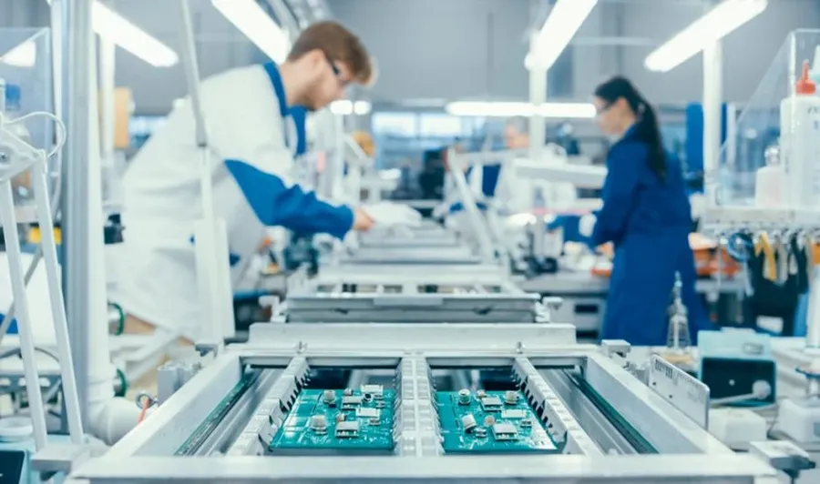
Manufacturing Capabilities and Technologies
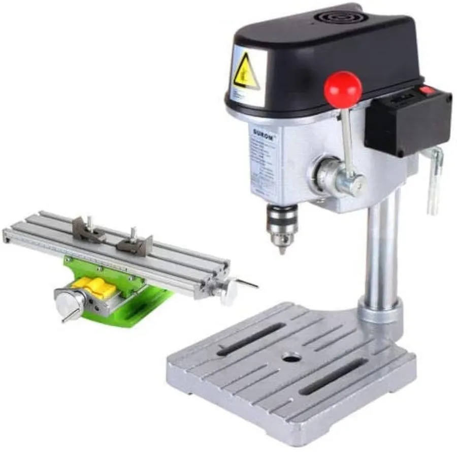
The fabrication of 16-layer PCBs demands sophisticated manufacturing processes and advanced technologies to ensure precision and reliability. These processes involve multiple steps, each critical to the final product's performance, including lamination, drilling, plating, and imaging. The complexity of these boards necessitates the use of state-of-the-art equipment and stringent quality controls to meet the demands of high-density, high-speed applications.
Here's a detailed look at the key manufacturing processes and technologies involved:
- Lamination
This process involves bonding multiple layers of prepreg (a fiberglass cloth impregnated with resin) and copper foil under heat and pressure. For 16-layer PCBs, this is a complex multi-step process requiring precise temperature and pressure control to avoid defects and ensure consistent layer adhesion. - Drilling
Precise drilling is essential for creating vias (interlayer connections) and component holes. Modern PCB manufacturers use Computer Numerical Control (CNC) drilling machines with laser alignment for accurate hole placement. For 16-layer boards, hole diameters and drill accuracy are critical for ensuring reliable connections between layers. - Plating
After drilling, the holes are plated with copper to create conductive pathways. This process involves electroless copper plating followed by electrolytic copper plating to build up the required thickness. Controlled plating thickness is crucial for impedance control and reliable signal transmission in multilayer PCBs. - Imaging
This step transfers the circuit pattern onto the copper layers using photoresist and UV light exposure. High-resolution imaging systems are essential for creating fine lines and spaces, which are often required for the high density of 16-layer boards. Accurate alignment of each layer is necessary to avoid shorts or opens.
Advanced technologies play a vital role in ensuring the quality of 16-layer PCBs:
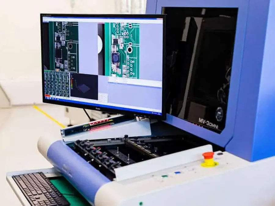
- Automated Optical Inspection (AOI)
AOI systems use cameras and sophisticated image processing software to automatically inspect PCBs for defects such as shorts, opens, and incorrect trace widths. This technology is crucial for identifying errors early in the manufacturing process, minimizing waste and improving yields, especially for complex multilayer PCBs. - X-ray Inspection
X-ray inspection is used to examine internal features of the PCB, such as buried vias and solder joints that are not visible through optical methods. This technology is critical for verifying the integrity of connections and identifying hidden defects in multilayer boards.
Key manufacturing capabilities related to 16-layer PCBs often include:
| Parameter | Typical Values for 16-Layer PCBs |
|---|---|
| Minimum Trace Width | 0.075 mm (3 mils) or less, depending on manufacturer capabilities. |
| Minimum Trace Spacing | 0.075 mm (3 mils) or less, depending on manufacturer capabilities. |
| Minimum Drill Hole Diameter | 0.2 mm (8 mils) or less for through-hole vias; 0.1mm or less for microvias |
| Maximum Panel Size | Varies by manufacturer; can be 18" x 24" or larger. |
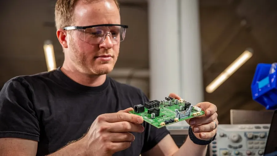
Quality Control and Certification
Rigorous quality control is paramount in the manufacturing of 16-layer PCBs, ensuring the reliability and performance required for complex electronic applications. This involves a multi-faceted approach encompassing process control, adherence to industry standards, and comprehensive testing procedures. Certifications from recognized bodies provide essential assurance of a manufacturer's commitment to quality.
The following certifications are critical for manufacturers of 16-layer PCBs:
- ISO 9001
This certification demonstrates a manufacturer's commitment to a quality management system. It ensures consistent processes and continuous improvement, which are critical for the complex manufacturing of multilayer PCBs. - IPC Standards
Adherence to IPC (Association Connecting Electronics Industries) standards ensures that PCBs meet industry-recognized quality and performance criteria. Specific IPC standards, such as IPC-A-600 for PCB acceptability and IPC-6012 for rigid PCB performance, are particularly important for high-layer-count PCBs. This include standards for via fabrication and trace geometry, which are crucial to ensuring performance of a 16-layer PCB. - UL Certification
Underwriters Laboratories (UL) certification indicates a product has met safety standards. For PCBs, this certification addresses materials, construction, and electrical safety, ensuring components are safe for use in electrical products. This is extremely important for reliability and safety for consumers.
Reliability testing is a crucial element of quality control, ensuring the longevity and stable operation of 16-layer PCBs. Manufacturers must use sophisticated testing procedures to identify potential weak points.
- Electrical Testing
This involves checking the electrical functionality of the board, including testing for opens, shorts, and correct component placement and connectivity. - Automated Optical Inspection (AOI)
AOI is used to identify visual defects such as shorts, opens, and misalignments using high-resolution cameras. This technology is critical for quality control of complex multilayer PCBs. - X-Ray Inspection
X-Ray inspection can reveal internal defects such as misaligned layers, void formation in vias, and incomplete solder joints. This is particularly important for multilayer boards where defects may not be visible on the surface. - Thermal Stress Testing
Subjecting the PCBs to extreme temperature variations to examine the durability of the PCB under thermal stress conditions to discover potential weak spots in materials or design that can lead to failure during temperature variation. - Impedance Testing
Verifying the impedance of the signal lines to ensure consistent signal performance is critical in high-speed applications. This test is crucial in the context of the precise routing required on a 16-layer board.
Cost and Turnaround Time
The cost and turnaround time for 16-layer PCB manufacturing are crucial considerations, heavily influenced by design complexity, material choices, production volume, and the manufacturer's capabilities. Balancing these factors is essential for meeting project deadlines and budgets.
Several factors contribute to the overall cost:
- Complexity of Design
More intricate designs with finer traces, smaller vias, and tighter spacing require more precision and time, increasing costs. Complex routing, blind and buried vias, and high-density interconnects significantly raise the price. - Materials
The type of materials used significantly impacts the final cost. High-Tg FR-4, specialized laminates, and materials with specific thermal and electrical properties are more expensive than standard FR-4. Material selection also affects the manufacturing process, further influencing price. - Quantity
The production volume also affects the per-unit cost. Larger production runs typically result in lower per-unit costs due to economies of scale. - Surface Finishes
Surface finishes like ENIG (Electroless Nickel Immersion Gold) are generally more expensive than HASL (Hot Air Solder Leveling). The choice of finish depends on performance requirements and cost considerations. - Testing Requirements
Comprehensive testing requirements such as impedance control, thermal and reliability tests, will increase costs.
Turnaround time, the time between order placement and delivery, is equally critical. Standard lead times for 16-layer PCBs are generally longer than for simpler boards, but can be shortened for a premium.
- Standard Lead Time
Typical lead times for 16-layer PCBs can range from 10 to 20 business days, depending on the manufacturer and complexity of the design. - Rush Order Options
Many manufacturers offer expedited services for urgent projects, which can significantly reduce lead times, but incur additional costs. Depending on the manufacturer capabilities, 16 layer PCBs can be produced in as little as 3-5 days for a premium.
To balance cost and time, consider the following:
- Planning Ahead
Allow ample time for manufacturing, including potential delays. Good project planning can reduce the need for costly rush orders. - Design Optimization
Optimize designs for manufacturability to reduce production time and cost. Minimize the use of complex design features and excessive layers where possible. - Material Considerations
Choose materials that balance performance requirements with budget constraints. Consider cost-effective alternatives without compromising essential qualities. - Negotiation and Collaboration
Communicate openly with manufacturers, seeking options to optimize costs and turnaround time while maintaining desired quality standards. - Quantity Evaluation
Accurately project quantity needs to achieve the best per unit price, which can reduce the overall project cost.
Frequently Asked Questions About 16 Layer PCB Manufacturing
This section addresses common queries regarding 16-layer PCB manufacturing, providing concise and authoritative answers to help clarify key aspects of this complex process.
- Who is the largest PCB manufacturer in the world?
Identifying the single largest PCB manufacturer is challenging due to fluctuating market share and varying metrics (e.g., revenue, production volume). However, companies like China-based Shennan Circuits and Taiwan-based Unimicron Technology are consistently ranked among the top global PCB manufacturers. - What exactly is a 16-layer PCB?
A 16-layer PCB is a printed circuit board comprising sixteen conductive layers, each separated by an insulating dielectric material. These layers are laminated together to form a single, integrated board. This configuration allows for complex signal routing, higher circuit density, and improved performance in high-speed electronic applications. - How many layers can a PCB have?
The number of layers in a PCB can range from a single layer to over 50, depending on the complexity and application requirements. Common configurations include single-layer, double-layer, and multilayer boards (e.g., 4, 6, 8, 10, 12, 16 layers and above). The practical limits are dictated by manufacturing capabilities and signal integrity considerations. - What are the common stack-up configurations for 16-layer PCBs?
Typical 16-layer PCB stack-ups include a combination of signal, ground, and power planes, strategically arranged to optimize signal integrity, minimize noise, and facilitate efficient power distribution. Common approaches involve placing ground planes adjacent to signal layers to control impedance, as well as separating high-speed signal layers from power planes. Exact configurations are often proprietary to the manufacturer and dependent on the board's intended use. - What are the primary materials used in 16-layer PCB manufacturing?
The most common material for 16-layer PCBs is FR-4, a fiberglass-reinforced epoxy laminate known for its good electrical and mechanical properties. However, for demanding applications, high-Tg FR-4 variants and specialized materials with enhanced thermal and electrical characteristics are utilized, such as polyimide, or PTFE-based laminates are used. - What is the typical lead time for manufacturing 16-layer PCBs?
Lead times for 16-layer PCB production vary depending on manufacturer capabilities, board complexity, and quantity of PCBs. Standard lead times may range from 2 to 6 weeks, while expedited options may reduce this to 1 to 2 weeks. Complex designs or large quantities often increase manufacturing times. - What are the critical factors impacting the cost of a 16-layer PCB?
The cost of 16-layer PCBs depends on a variety of factors including materials used (especially the choice of dielectric material), the complexity of the design (trace widths and spacing, vias, etc.) , the required surface finishes, and the production volume. High-Tg materials and fine-pitch designs significantly increase costs. As does the use of impedance controlled traces.
Working with a 16 Layer PCB Manufacturer
Effective communication and clear documentation are paramount when collaborating with a 16-layer PCB manufacturer. This ensures that the final product meets the design specifications, functional requirements, and performance criteria necessary for your project. A robust communication strategy minimizes errors, reduces delays, and optimizes the manufacturing process.
- Clear Design Files (Gerber)
Gerber files are the industry-standard format for PCB manufacturing. These files contain all necessary information about the board's layers, traces, pads, and vias. Ensure that your Gerber files are complete, accurate, and use the correct naming conventions as requested by the manufacturer. Include a comprehensive Readme file specifying the layer stackup, material requirements, and any special fabrication notes. - Design Rule Checks (DRC)
Before submitting your design, it's critical to perform thorough Design Rule Checks (DRC). DRC ensures that your design adheres to the manufacturer's capabilities regarding minimum trace widths, spacing, via sizes, and other critical parameters. This proactive step can identify potential manufacturability issues early on, preventing costly revisions and delays in the manufacturing process. Address any violations before sending the files to the manufacturer. - Communication Channels
Establish clear channels of communication with the manufacturer from the beginning. Designate a primary point of contact on both sides. Use email, phone, or project management platforms as needed. Timely and accurate communication ensures that you get quick responses to questions, and timely resolution to any problems that might arise. - Addressing Design Issues
Be prepared to discuss potential design issues with the manufacturer. They may identify areas where your design could be improved for manufacturability or performance. Be open to suggestions and work together to find practical, cost-effective solutions. Document all changes and communicate them promptly to the design and manufacturing team. - Understanding the Manufacturer's Capabilities
Before starting the design, ensure the manufacturer is capable of producing your specific 16 layer design. Understand their minimum trace width and spacing, drilling capabilities, materials they support, and available surface finishes to make sure your design is compatible and achievable. This helps avoid design iterations and rework during the process.
Choosing the right 16 layer PCB manufacturer is a pivotal decision for any high-stakes project. By focusing on a manufacturer's expertise, materials, manufacturing process, and quality control, you're setting the stage for optimal performance and long-term success. Always prioritize clear communication and a collaborative relationship with your chosen partner. Whether you're building complex medical devices or groundbreaking AI systems, a dependable and skilled 16 layer PCB manufacturer is your gateway to innovation. Consider this guide as your starting point, and take the necessary steps to connect with a qualified supplier who can meet your exact project requirements.