Choosing the Right Double Sided PCB Manufacturer: A Comprehensive Guide
In today's fast-paced electronics industry, double sided PCBs are fundamental components in countless devices. From consumer gadgets to sophisticated industrial machinery, these boards form the backbone of modern technology. Choosing the right double sided PCB manufacturer is not just about finding a supplier; it's about securing a partner who can deliver quality, reliability, and value. This article dives into the key factors to consider when selecting a manufacturer, helping you make informed decisions and ensuring your project's success.
Understanding Double Sided PCBs
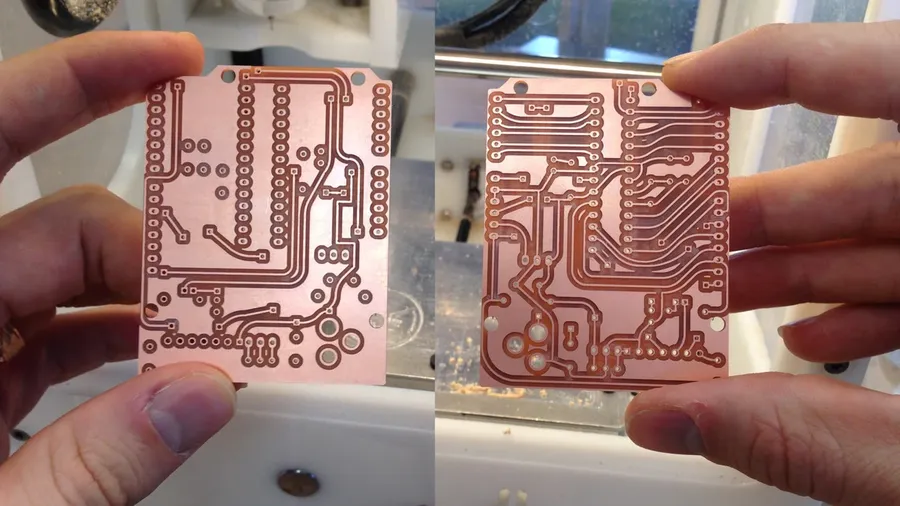
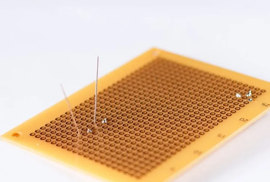
Double-sided PCBs are a fundamental component in modern electronics, distinguished by their conductive copper layers on both sides of the substrate, allowing for more complex circuitry and greater component density than their single-sided counterparts. This design enables more intricate routing and reduces board size, making them a versatile choice for a wide array of applications.
Unlike single-sided PCBs, which have conductive paths on only one side, double-sided PCBs utilize both sides, significantly increasing the surface area available for component placement and signal routing. This structure allows for more intricate circuit designs and efficient signal management. Compared to multi-layer PCBs, double sided PCBs are generally more cost-effective for designs that require medium complexity, without the need for multiple internal layers for signals and power.
- Advantages of Double-Sided PCBs:
Higher component density, more complex routing options, reduced board size, and better cost-effectiveness for medium-complexity designs. - Disadvantages of Double-Sided PCBs:
Limited to two layers and therefore less dense compared to multi-layer boards, may require through-hole technology for certain interconnections which could increase board space requirements. - Common Applications of Double-Sided PCBs:
Consumer electronics (such as appliances, computers, and mobile phones), industrial control systems, automotive electronics, communication devices, and basic power supplies.
| Feature | Single-Sided PCB | Double-Sided PCB | Multi-Layer PCB |
|---|---|---|---|
| Conductive Layers | One | Two | Three or more |
| Complexity | Low | Medium | High |
| Cost | Lowest | Medium | Highest |
| Component Density | Low | Medium | Highest |
| Applications | Simple electronics, basic circuits | Consumer electronics, industrial control systems | High-end electronics, advanced applications |
Key Considerations When Choosing a Double Sided PCB Manufacturer
Selecting the right double-sided PCB manufacturer is crucial for ensuring the success of your electronic projects. This decision hinges on several key factors, each impacting the final product's quality, cost, and delivery timeline. A thorough evaluation of a manufacturer's capabilities, material options, certifications, and turnaround times is essential to meet specific project requirements and avoid costly setbacks.
- Manufacturing Capabilities
Assess the manufacturer's capacity to produce PCBs that meet your design specifications. This includes minimum trace widths and spacing, hole sizes, and board dimensions. Verify their equipment and technology can accommodate your design’s complexity and quantity needs, ranging from small prototypes to large-scale production runs. - Material Options
Explore the available substrate materials, such as FR-4, CEM-1, or polyimide, considering their thermal, mechanical, and electrical properties to suit your application. Pay particular attention to copper thickness, which affects current-carrying capacity and signal integrity, and surface finishes (e.g., HASL, ENIG, OSP), which impact solderability and corrosion resistance. The right material choice is critical for performance and reliability. - Quality Certifications (ISO, UL)
Confirm that the manufacturer holds relevant certifications, such as ISO 9001 for quality management and UL certifications for product safety. These certifications demonstrate adherence to industry standards and provide assurance of consistent quality and manufacturing processes. It's important to select a manufacturer that can provide traceable, standardized processes. - Turnaround Times
Evaluate the manufacturer’s lead time from design submission to delivery. Consider your project timeline and the manufacturer's ability to meet your deadlines, including any prototyping or revision cycles. Inquire about their rush service options if expedited production is crucial, understanding the trade-offs between speed and potential cost implications.
Manufacturing Processes Explained
The fabrication of double-sided PCBs involves a multi-stage process, transforming a design concept into a functional electronic component. This process encompasses several key steps, from initial design and material preparation to final assembly and testing. A thorough understanding of these processes is essential for ensuring the quality and reliability of the final product.
The manufacturing of double-sided PCBs follows a structured sequence of operations, which can be broadly categorized into the following:
- Design and Layout
The process begins with the design and layout of the circuit using CAD software. This step involves defining the component placement, trace routing, and overall board dimensions. The design data is then translated into a format suitable for manufacturing. - Material Selection
Based on the performance and application requirements, appropriate base materials are chosen. These materials typically include a dielectric substrate (usually fiberglass-reinforced epoxy resin) and copper cladding. The choice of materials influences the electrical and mechanical properties of the final PCB. - Layer Imaging
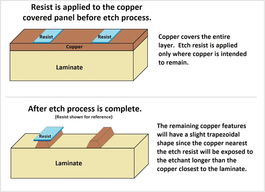
The copper layers are coated with a photosensitive resist. The circuit pattern is then transferred onto the copper using UV light exposure through a photomask. The exposed resist hardens, while the unexposed areas remain soluble. - Etching
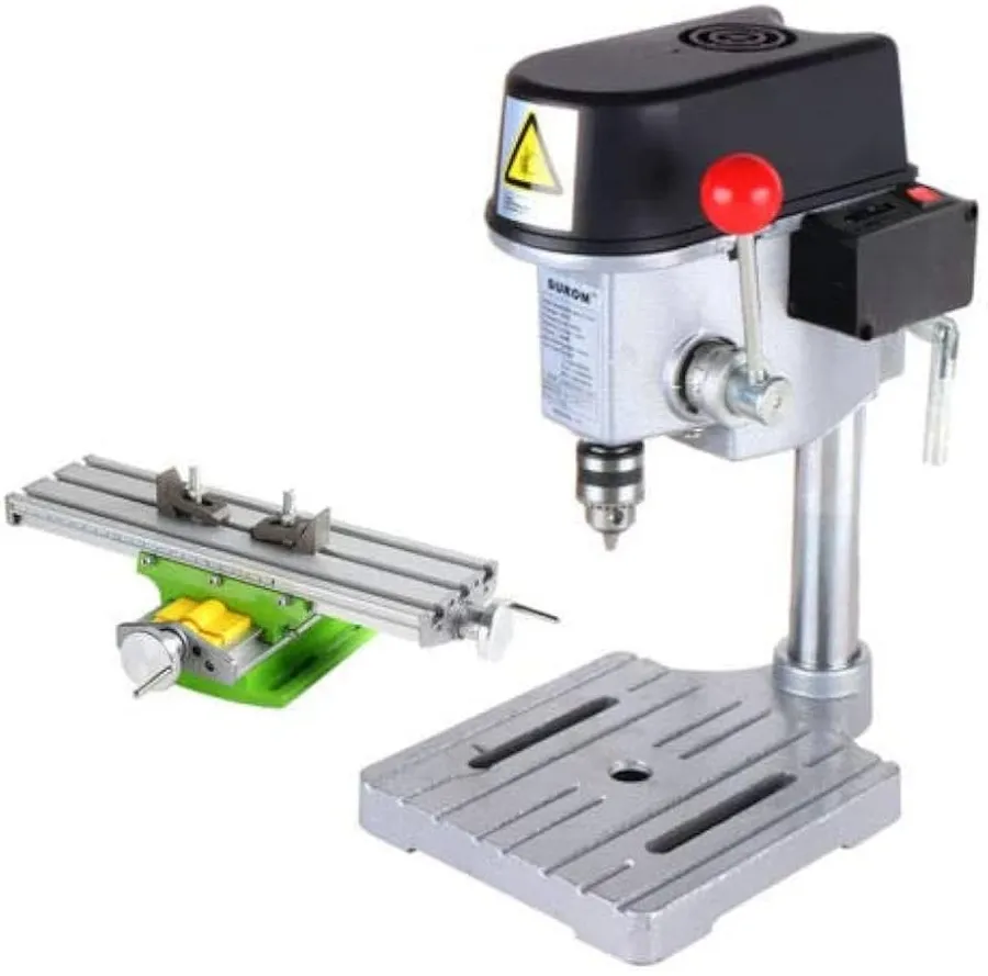
The unexposed resist is washed away, and the underlying copper is removed using a chemical etchant, leaving the desired copper traces. This process defines the conductive pathways on both sides of the PCB. - Drilling
Holes for through-hole components and vias (conductive pathways between layers) are precisely drilled using automated drilling machines. Drill size and location are critical for ensuring reliable connections. - Plating
A thin layer of copper is deposited onto the hole walls through an electroplating process. This creates conductive pathways between the two sides of the PCB and ensures electrical connection to components. - Solder Mask Application
A solder mask (usually a green epoxy coating) is applied to the entire board, except for the pads and through-hole areas that are to be soldered. This mask protects the board from oxidation and prevents solder bridges during assembly. - Surface Finish Application
A surface finish, such as HASL, ENIG, or immersion silver, is applied to the exposed copper pads. This finish protects the copper from oxidation and ensures good solderability. - Silkscreen Application
Silkscreen printing is used to apply component designators, logos, and other markings to the board. This aids in component placement during assembly and facilitates board identification. - Final Testing and Inspection
The finished PCBs are subjected to rigorous testing and visual inspection to ensure they meet the design specifications. Tests include electrical continuity checks, shorts detection, and dimensional verification.
These processes form the backbone of double-sided PCB manufacturing, resulting in a finished product ready for component assembly. Two key assembly technologies are pivotal in this stage:
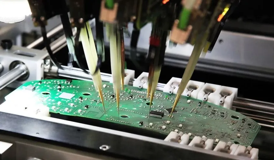
- Surface Mount Technology (SMT)
SMT involves placing components directly on the surface of the PCB. This technology is ideal for high-density circuit designs and automated assembly. - Through-Hole Technology (THT)
THT involves inserting components into pre-drilled holes on the PCB and soldering them in place. This technique is often used for larger components that require stronger mechanical connections.
Cost Factors in Double Sided PCB Manufacturing
The cost of manufacturing double-sided PCBs is influenced by a variety of interconnected factors. These range from the raw materials and design complexity to production volume and lead times. A thorough understanding of these elements is crucial for effective cost management and achieving the optimal balance between cost and quality.
| Cost Factor | Description | Impact on Cost |
|---|---|---|
| Material Selection | The choice of substrate material (e.g., FR-4, Rogers), copper thickness, and surface finish. | Higher performance materials and thicker copper generally increase costs. |
| Design Complexity | Number of layers, trace width and spacing, via count, and overall board size. | More complex designs with finer features require advanced manufacturing processes and increase cost. |
| Order Volume | Quantity of PCBs produced in a single order. | Larger production runs benefit from economies of scale, reducing per-unit costs. |
| Lead Time | The time required from design submission to final delivery. | Expedited or rush orders typically incur additional costs. |
| Surface Finish | Type of surface finish selected, such as HASL, ENIG, or OSP. | Specialized finishes such as ENIG are more expensive than standard finishes such as HASL. |
| Testing Requirements | Specific testing needs including impedance control, continuity testing, or other advanced testing methods. | Advanced testing can be complex and will increase cost of production. |
Effective cost management in double-sided PCB manufacturing requires a careful approach. Strategies should focus on optimizing the design, selecting appropriate materials and finishes, consolidating orders where possible, and maintaining a realistic lead time.
- Design Optimization for Cost Reduction:
Simplifying the layout of your PCB reduces the complexity of the manufacturing process. Use wider traces and spaces where possible, limit via count, and avoid unnecessarily small or complex features. This can significantly impact cost without compromising essential functions. - Material Choice:
Where possible, use standard materials such as FR-4 for the substrate and HASL for the finish, this is a standard production method and is generally cost effective. Avoid specialized or high performance materials if they do not provide the needed level of performance for the intended application. - Consolidation of Orders:
Combining multiple PCB projects or anticipating future needs to create larger orders can help reduce the per-unit cost through economies of scale. Check with your manufacturer for pricing discounts with volume production. - Realistic Lead Time:
Planning for sufficient manufacturing lead time reduces the need for expensive rush services. Early communication with your chosen manufacturer about your timelines can be a helpful strategy to reduce costs.
Prototyping and Small Batch Runs for Double Sided PCBs
Prototyping and small batch runs are critical stages in the development of double-sided PCBs, allowing for design validation and iterative improvement before committing to large-scale production. These initial runs serve to identify and rectify any design flaws, material issues, or manufacturing inconsistencies, ensuring a more efficient and cost-effective mass production process. Manufacturers specializing in these services offer valuable support during the crucial early phases of product development.
Key aspects to consider when evaluating a manufacturer's capabilities in prototyping and small batch runs include:
- Design for Manufacturability (DFM) Support:
Assess if the manufacturer offers DFM feedback, which helps in optimizing the PCB design for efficient manufacturing processes. DFM analysis can reveal potential issues related to component placement, trace width and spacing, via design, and other design considerations that may affect manufacturing yields and product performance. - Rapid Turnaround Times:
Quick turnaround times are crucial in prototyping to expedite development cycles. Manufacturers that can produce prototypes in a short timeframe allow for quicker design iterations and faster time-to-market. - Minimum Order Quantity (MOQ) Flexibility:
For prototype and small batch orders, low MOQs are desirable. Manufacturers should be flexible in accommodating low volumes without disproportionately increasing per-unit costs. This allows for experimentation and testing at lower investment costs. - Material Selection:
Manufacturers should offer a variety of materials suitable for prototyping and small runs, allowing for testing different material characteristics in real world applications, such as different types of FR-4, or materials with specific dielectric or thermal properties. The material choices at this stage should be similar to that planned for mass production to evaluate the true effect of these materials on final product. - Assembly Services:
If component assembly is part of the prototyping plan, ascertain if the manufacturer can offer this as part of the small-batch service, as this can shorten the time from initial production to functional prototype. - Prototyping Techniques:
The manufacturer's technology should support a range of prototyping and assembly methods, such as surface mount technology (SMT) and through-hole technology (THT), to ensure prototypes accurately reflect the final product.
Selecting a manufacturer with proven experience in prototyping and small batch production is essential to successfully transition from design to production. This approach reduces risks, and provides the opportunity to optimize both design and manufacturing process.
Quality Assurance and Testing
Rigorous quality assurance and testing are paramount in the manufacturing of double-sided PCBs to ensure their reliability and performance. These processes identify potential defects and verify adherence to design specifications, ultimately reducing the risk of product failure.
Several key tests are employed in the quality control of double-sided PCBs:
- Impedance Control Testing
This test verifies that the characteristic impedance of signal traces on the PCB meets the design specifications. Impedance mismatches can cause signal reflections and losses, leading to performance issues. Time-domain reflectometry (TDR) is a common method for this testing. - Continuity Testing
This ensures that all electrical connections are correctly made and that there are no opens or shorts in the circuit paths. Automated testing systems or manual multimeters can perform this type of test, where each net is tested for continuity based on the board's netlist. - Short Circuit Testing
This testing is performed to ensure that unintended electrical connections (shorts) between different nets do not exist on the circuit board. Short circuits can cause electrical faults, overheating, and even complete failure of the electronic device. - Dielectric Withstand Testing
This test measures the capacity of the PCB's insulating material to resist electrical breakdown under high voltage. The test voltage is significantly higher than the intended operating voltage, ensuring the PCB can withstand high voltage without causing arc-over or insulation failure. - Solderability Testing
This test confirms that the PCB surface is suitable for soldering, ensuring that components can be reliably soldered to the pads. This test typically includes 'dip and look', 'wetting balance' and 'solder float' test, and determines whether the solder pads and through-holes of a PCB will allow for good solder flow. - X-Ray Inspection
X-ray inspection is a non-destructive testing method used to look for defects in the inner layers of the multilayer PCBs, component alignment, solder joints, and other hidden features. The X-Ray can penetrate different layers of materials and generate images based on density variations. - Automated Optical Inspection (AOI)
This automated inspection method utilizes a camera to capture images of the PCB to compare with the reference board design, highlighting anomalies such as shorts, open circuits, missing pads, incorrect components, etc.
In addition to these tests, it is crucial that a double-sided PCB manufacturer holds specific certifications to demonstrate commitment to quality:
- ISO 9001
This is a generic international standard that specifies requirements for a quality management system (QMS), demonstrating the manufacturer's ability to consistently provide products that meet customer and regulatory requirements. - UL Certification
Underwriters Laboratories (UL) certification ensures that PCBs meet recognized safety standards and compliance, essential for product safety and reliability. - IPC Standards
Compliance with IPC (Association Connecting Electronics Industries) standards such as IPC-A-600 (Acceptability of Printed Boards) and IPC-6012 (Qualification and Performance Specification for Rigid Printed Boards) indicates adherence to industry best practices for PCB manufacturing and assembly, quality, and inspection.
Selecting a manufacturer that employs rigorous testing methodologies and holds relevant certifications is critical for ensuring the production of high-quality, reliable double-sided PCBs.
Frequently Asked Questions About Double Sided PCB Manufacturing
This section addresses common questions regarding double-sided PCB manufacturing, providing clear and concise answers to guide you through the process and considerations involved.
- How are double-sided PCBs manufactured?
Double-sided PCBs are manufactured through a multi-step process that includes design, printing the circuit onto a laminate, etching away excess copper, drilling holes for vias and components, plating the vias, applying solder mask, and screen printing the silkscreen. The process involves precision in each step to ensure the circuit's integrity. - Who are some of the leading double-sided PCB manufacturers?
The leading double-sided PCB manufacturers vary geographically and in specialization. However, some well-regarded manufacturers are known for their quality and reliability, often being selected based on project requirements. It's best to search by region and specializations as needs vary significantly, and referencing industry publications may provide a more specific list of leading manufacturers. Research and compare manufacturers by their certifications, material capabilities, and process technology, which is critical when evaluating potential partners. - What are the two sides of a PCB called?
The two sides of a double-sided PCB are typically referred to as the 'top' (or component side) and the 'bottom' (or solder side). The component side generally houses the components, while the solder side is where solder connections are made. These terms are used universally in PCB design and assembly. - What materials are commonly used in double-sided PCB production?
Common materials include FR-4 (a flame-retardant glass epoxy laminate), copper (for conductive layers), solder mask (to protect the copper), and silkscreen ink (for component identification). Copper thickness and finishes also vary based on the application. FR-4 is often favored for its good balance of cost, electrical performance, and mechanical stability, though more specialized materials can be used for demanding applications. - How can I optimize my PCB design for cost-effective production?
To optimize for cost-effective production, consider reducing board complexity, using standard component sizes and footprints, minimizing the number of layers and vias, avoiding unnecessary features and specifying tolerances only where necessary. Furthermore, consulting with the manufacturer early on in the design phase can help identify any additional cost drivers and optimize your designs for their fabrication process. - What is the difference between rigid and flex PCBs?
Rigid PCBs, like the double-sided PCB, are made from inflexible materials like FR-4 and are designed for applications that do not require bending. Flex PCBs, in contrast, are made from flexible substrates like polyimide and are designed to be bent or flexed without damage, allowing for unique designs and space constraints. These distinct differences suit unique applications and demands, making the selection a critical step in any electronics design. - What are the key differences between Single-Sided, Double-Sided, and Multilayer PCBs?
Single-sided PCBs have conductive traces on only one side of the board. Double-sided PCBs have traces on both sides, connected by vias. Multilayer PCBs have three or more layers of conductive traces. Single-sided PCBs are the simplest and cheapest to manufacture but are the most limited in terms of circuit complexity. Double-sided PCBs offer more design flexibility, and multilayer PCBs can handle very complex circuitry. The increased complexity is associated with increased cost.
Comparing Double Sided PCB Manufacturers: Key Metrics
Selecting the right double-sided PCB manufacturer involves a careful evaluation of several key metrics. This section provides a structured approach to comparing manufacturers based on crucial factors, enabling informed decisions aligned with project requirements and priorities. We'll explore critical elements such as material capabilities, turnaround times, cost structures, and service offerings, highlighting the advantages and disadvantages of each.
| Metric | Description | Small Batch Focus | Mass Production Focus | Considerations |
|---|---|---|---|---|
| Material Capabilities | Range of materials supported, including copper thickness, base material types (e.g., FR-4, Aluminum, Rogers), and surface finishes (e.g., HASL, ENIG, Immersion Silver). | May offer a wider range of material options for design flexibility. | Standard materials are often readily available, allowing for reduced costs and quicker delivery. | Ensure the manufacturer can support your required specifications. |
| Turnaround Time | The time required from design submission to delivery of finished PCBs. Includes prototyping and production lead times. | Fast turnarounds are often crucial; may have premium pricing. | Longer lead times for cost optimization and batch processing. | Plan for your needs and how they may impact your project timelines. |
| Cost Structure | Pricing models based on volume, material, design complexity, and additional services like testing. Includes tooling costs, setup fees and per unit price. | May offer lower setup costs and flexible per-unit pricing. | Lower per unit cost are typical for large-scale volumes. | Evaluate the overall cost for your volume needs. |
| Quality Standards and Certifications | The level of quality assurance measures and industry certifications such as ISO 9001, UL certifications, and IPC standards. | May be flexible with certifications for the production of prototype batches. | Often meet stricter regulatory compliance. | Consider which certifications and standards are most important for your product. |
| Service Offerings | Includes options for design support, prototype runs, small to large volume manufacturing, testing, assembly, and logistics. | More personalized service, with the ability to adjust requirements on the fly. | Standardized workflows with scalable solutions. | Identify if you will require additional services like design, assembly, etc. |
Future Trends in Double Sided PCB Technology
The landscape of double-sided PCB technology is continuously evolving, driven by demands for higher performance, miniaturization, and sustainability. Innovations in materials, fabrication techniques, and market trends are shaping the future of PCB manufacturing. These advancements promise to enhance product functionality, reduce manufacturing costs, and improve environmental impact.
- Materials Innovations
Emerging materials are being developed to enhance the performance and reliability of double-sided PCBs. These include: * **High-performance laminates:** Offering improved thermal management and electrical properties. * **Environmentally friendly materials:** Bio-based and recyclable materials that reduce the environmental footprint of PCB production. * **Advanced dielectrics:** Enabling higher signal speeds and lower losses. - Advanced Fabrication Techniques
Cutting-edge fabrication techniques are revolutionizing double-sided PCB manufacturing: * **Additive manufacturing (3D printing):** Enables faster prototyping and customized designs with greater flexibility. * **Laser Direct Structuring (LDS):** Allows for precise placement of conductive traces, reducing waste and improving circuit density. * **Micro-via technology:** Facilitating high-density interconnects for miniaturized electronic devices. - Market Trends and Future Directions
The market is shifting towards: * **Increased demand for flexible PCBs:** Meeting the need for wearable electronics and flexible display technologies. * **Greater focus on sustainability:** Driving the adoption of eco-friendly materials and production processes. * **Integration of smart capabilities:** Incorporating sensors and communication modules directly into PCBs.
These trends are not only advancing the capabilities of double-sided PCBs but are also influencing the entire electronics industry, enabling the development of innovative products and applications. Staying abreast of these developments is crucial for manufacturers and designers alike.
Choosing the right double sided PCB manufacturer is a critical decision that can significantly impact the success of your electronic projects. By understanding the nuances of PCB manufacturing, assessing your specific needs, and carefully comparing different manufacturers, you can secure a reliable partnership that will deliver quality and value. As technology advances, staying informed about future trends in PCB manufacturing will be critical in maintain a competitive edge. Partnering with a reputable manufacturer like [double sided pcb manufacturer] can help navigate these changes and ensure consistent high-quality results.